

Light emitting device, light emitting device package including the device, and lighting apparatus including the package
a technology of light emitting devices and light emitting devices, which is applied in the direction of basic electric elements, electrical equipment, semiconductor devices, etc., can solve problems such as various problems
Active Publication Date: 2018-04-19
SUZHOU LEKIN SEMICON CO LTD
View PDF0 Cites 4 Cited by
- Summary
- Abstract
- Description
- Claims
- Application Information
AI Technical Summary
Benefits of technology
The light emitting device and package described in this patent use a metal reflecting layer to improve luminous flux, solve manufacturing issues with distributed Bragg reflector, and improve heat release characteristics. The metal reflecting layer reflects light and serves as a field plate, preventing damage from high electric fields. Overall, this technology makes lighting apparatus more efficient and reliable.
Problems solved by technology
At this time, various problems may arise due to the use of the DBR.
Method used
View moreImage
Smart ImageViewing Examples

Examples
Embodiment Construction
[0137]Various embodiments have been described in the best mode for carrying out the invention.
INDUSTRIAL APPLICABILITY
[0138]The light emitting device and the light emitting device package including the device according to the embodiment may be not broken at a high electric field by serving the metal reflecting layer as a field plate and applied to the display apparatus, the indicator apparatus, and the lighting apparatus having the improved thermal release characteristics.
Login to View More PUM
 Abstract
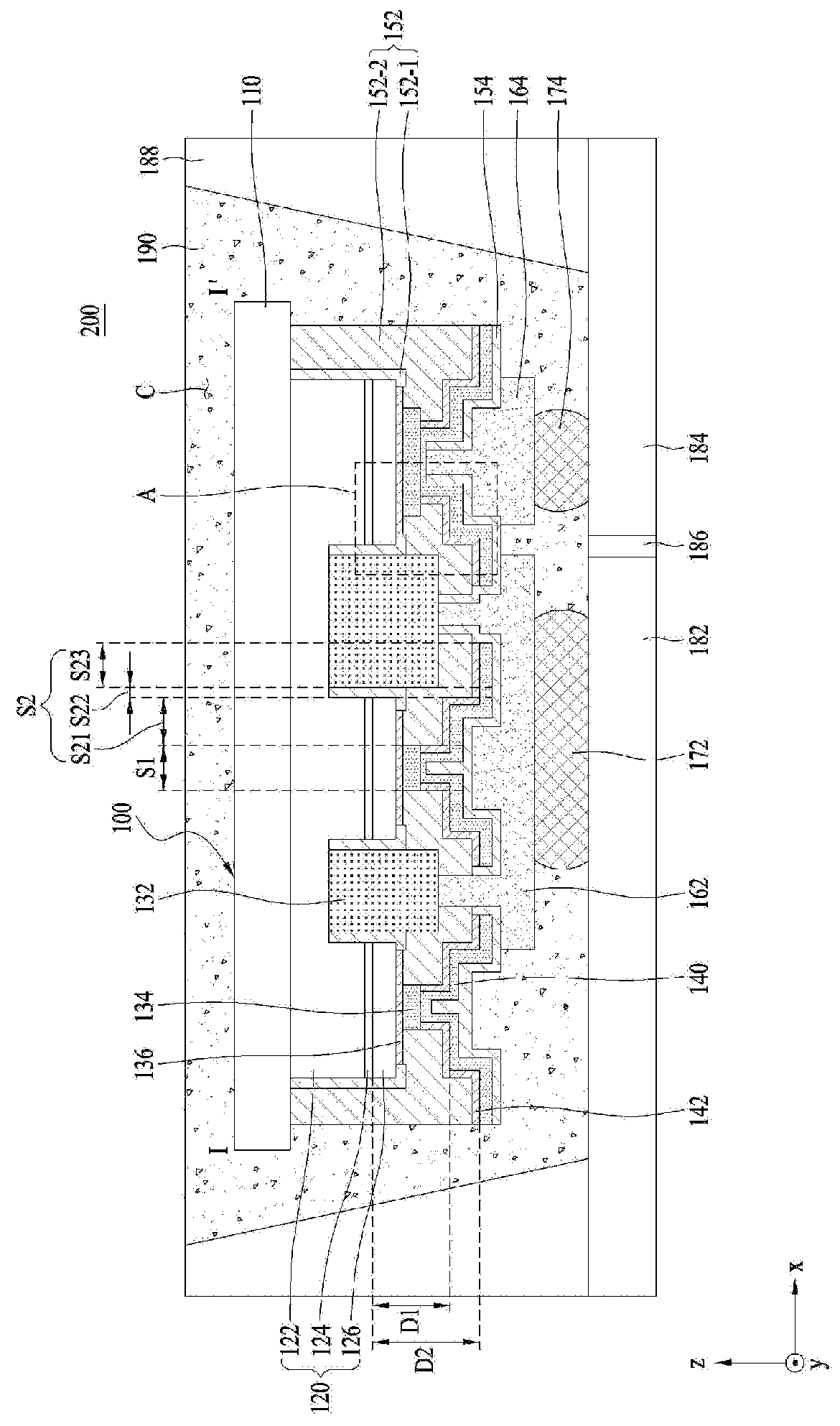
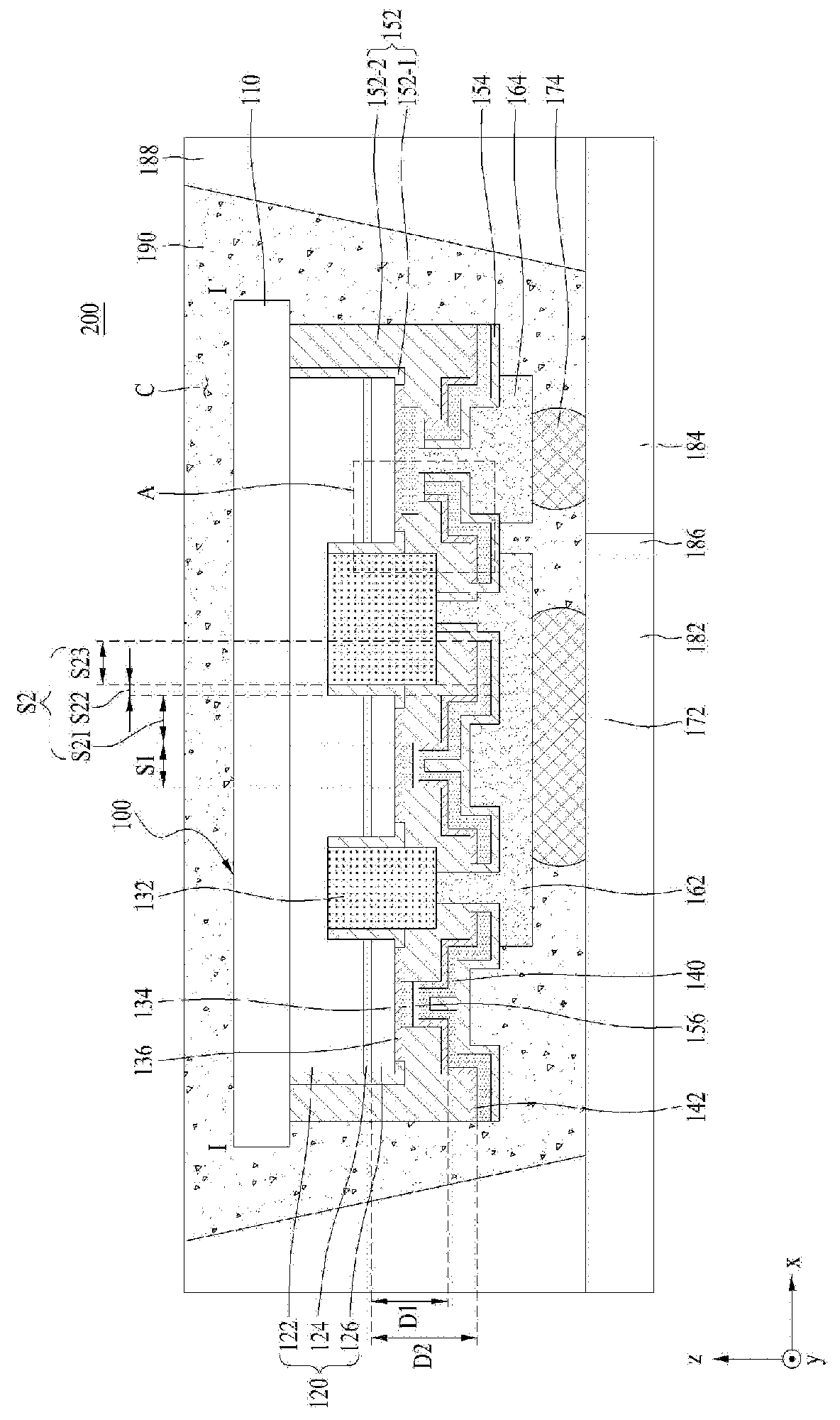
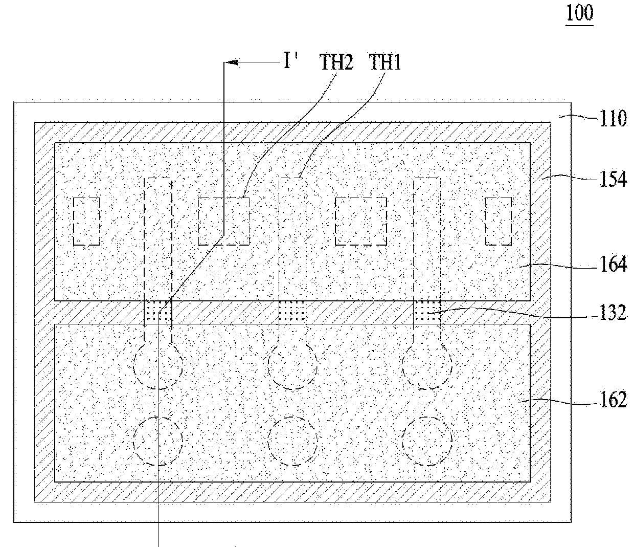
A light emitting device of an embodiment includes a substrate, a light emitting structure disposed under the substrate, the light emitting structure including a first conductive semiconductor layer, an active layer, and a second conductive semiconductor layer, first and second electrodes respectively connected to the first and second conductive semiconductor layers, a metal reflecting layer disposed under the light emitting structure, and a first insulating layers disposed between the first electrode and the light emitting structure, between the first electrode and the second electrode, and between the first electrode and the metal reflecting layer, wherein the metal reflecting layer includes a first segment overlapped with the second electrode in a thickness direction of the light emitting structure and a second segment disposed with extending from the first segment.
Description
TECHNICAL FIELD[0001]Embodiments relate to a light emitting device, a light emitting device package including the device, and a lighting apparatus including the package.BACKGROUND ART[0002]Light Emitting Diodes (LEDs) are semiconductor devices that convert electricity into light using characteristics of compound semiconductors so as to enable transmission / reception of signals, or that are used as a light source.[0003]Group III-V nitride semiconductors are in the spotlight as core materials of light emitting devices such as, for example, LEDs or Laser Diodes (LDs) due to physical and chemical characteristics thereof.[0004]The LEDs do not include environmentally harmful materials such as mercury (Hg) that are used in conventional lighting appliances such as, for example, fluorescent lamps and incandescent bulbs, and thus are very eco-friendly, and have several advantages such as, for example, long lifespan and low power consumption. As such, conventional light sources are being rapidl...
Claims
Login to View More Application Information
Patent Timeline
 Patent Type & AuthorityApplications(United States)
IPC IPC(8): H01L33/40H01L33/42H01L33/38H01L33/44
CPCH01L33/405H01L33/42H01L33/382H01L33/44H01L2933/0016H01L33/62H01L33/32H01L33/0025H01L33/46
InventorJUNG, SUNG HOCHOI, JIN KYUNGLEE, SANG YOUL
OwnerSUZHOU LEKIN SEMICON CO LTD