

Space-through charge transfer compound, and organic light emitting diode and organic light emitting display device including the same
a charge transfer compound and charge transfer technology, applied in the field of emitting materials, can solve the problems of not meeting the requirements of emitting efficiency and reliability, and achieve the effect of improving emission efficiency and high emitting efficiency
Pending Publication Date: 2019-12-05
LG DISPLAY CO LTD
View PDF1 Cites 0 Cited by
- Summary
- Abstract
- Description
- Claims
- Application Information
AI Technical Summary
Benefits of technology
The technical effect of this patent is to provide a space-through charge transfer compound with high emitting efficiency. This compound can be used in OLED displays and organic light emitting displays to improve their emission efficiency.
Problems solved by technology
However, there is no blue phosphorescent compound meeting the requirements in emitting efficiency and reliability.
Method used
View moreImage
Smart ImageViewing Examples

Examples
example 1 (
Ex1)
[0079]The compound 1 in Formula 6 is used as the dopant in the emitting material layer.
example 2 (
Ex2)
[0080]The compound 13 in Formula 6 is used as the dopant in the emitting material layer.
example 3 (
Ex3)
[0081]The compound 8 in Formula 6 is used as the dopant in the emitting material layer.
Login to View More PUM
| Property | Measurement | Unit |
|---|---|---|
| energy level | aaaaa | aaaaa |
| LUMO | aaaaa | aaaaa |
| charge transfer | aaaaa | aaaaa |
Abstract
The present disclosure provides a space-through charge transfer compound of following formula and an organic light emitting diode and an organic light emitting display device including the space-through charge transfer compound.
Description
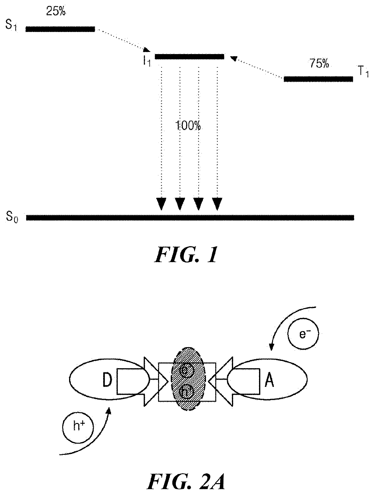
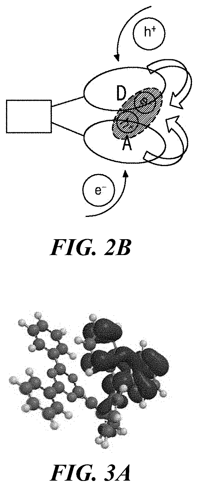
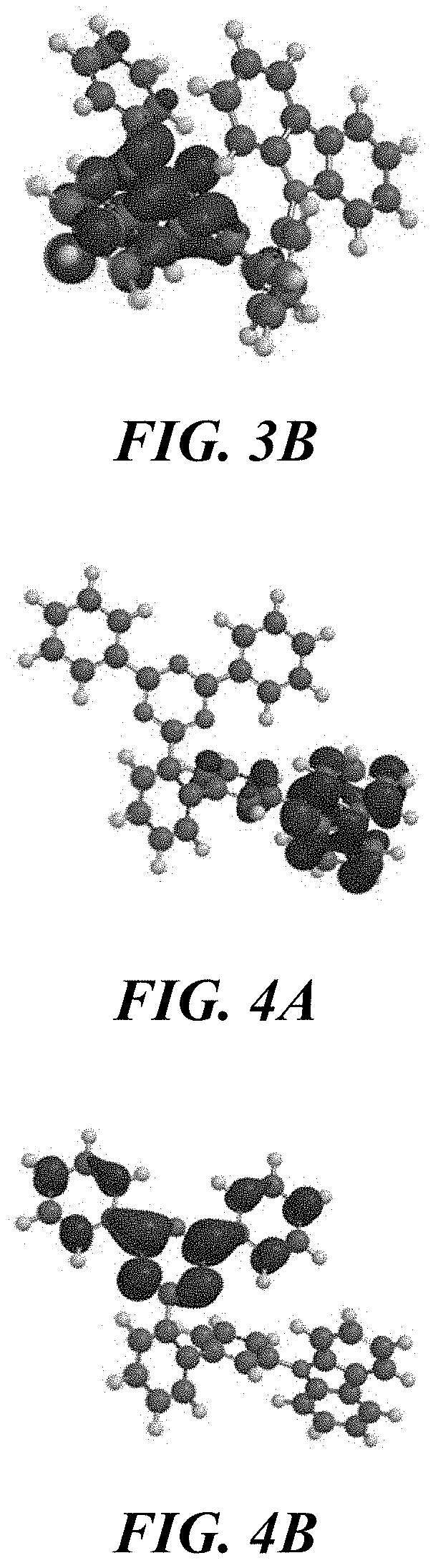
CROSS-REFERENCE TO RELATED APPLICATIONS[0001]This application claims priority to and the benefit of Republic of Korea Patent Application No. 10-2018-0063614 filed on Jun. 1, 2018, which is hereby incorporated by reference in its entirety.BACKGROUNDTechnical Field[0002]The present disclosure relates to an emitting material and more particularly to a space-through charge transfer compound having excellent emitting efficiency and an organic light emitting diode (OLED) and an organic light emitting display device including the space-through charge transfer compound.Description of the Related Art[0003]The requirements of the large-size display device have led to developments in flat panel display devices as an image displaying device. Among the flat panel display devices, the OLED has rapidly developed.[0004]In the OLED, when the electron from a cathode, which serves as an electron-injecting electrode, and the hole from an anode, which serves as a hole-injecting electrode, are injected i...
Claims
Login to View More Application Information
Patent Timeline
 Patent Type & AuthorityApplications(United States)
IPC IPC(8): H01L51/00C09K11/06C09K11/02C07D403/10H10K99/00
CPCH01L51/5004C09K2211/1007H01L51/5088H01L51/5072C09K2211/1018C09K11/02H01L51/0072H01L51/5016H01L51/5096H01L51/5092C09K11/06H01L51/5056H01L2251/552C07D403/10H01L51/0067C07D491/107C07D403/14C07D401/10C09K2211/1029C09K2211/1044C09K2211/1088C09K2211/1059H10K85/654H10K85/657H10K85/6572H10K50/11H10K50/181H10K50/18H10K50/84H10K50/15H10K50/16H10K50/17H10K50/171H10K2101/10H10K2101/30H10K2101/40
InventorNOH, HYO-JINYOON, KYUNG-JINSEO, BO-MIN
OwnerLG DISPLAY CO LTD