Unlock instant, AI-driven research and patent intelligence for your innovation.

Image display device

a technology of image display and display screen, which is applied in the direction of lighting and heating equipment, television systems, instruments, etc., can solve the problems of reducing and achieve the effect of improving the utilization efficiency of lights

Inactive Publication Date: 2007-06-19
MAXELL HLDG LTD
View PDF2 Cites 21 Cited by
  • Summary
  • Abstract
  • Description
  • Claims
  • Application Information

AI Technical Summary

Benefits of technology

The present invention provides an image display device that enhances the utilization efficiency of lights. This is achieved by using a light source with multiple semiconductor light-emitting elements, a parallelizing unit with multiple cell lenses, an image display element, and a projection unit. The semiconductor light-emitting elements are located at the focal points of the cell lenses, and there are at least two types of semiconductor light-emitting elements' groups with different optical axes. This results in improved light utilization and better image quality.

Problems solved by technology

This results in a problem that utilization efficiency of lights will be reduced.

Method used


Image

  • Image display device
  • Image display device
  • Image display device

Examples


first embodiment

[First Embodiment]

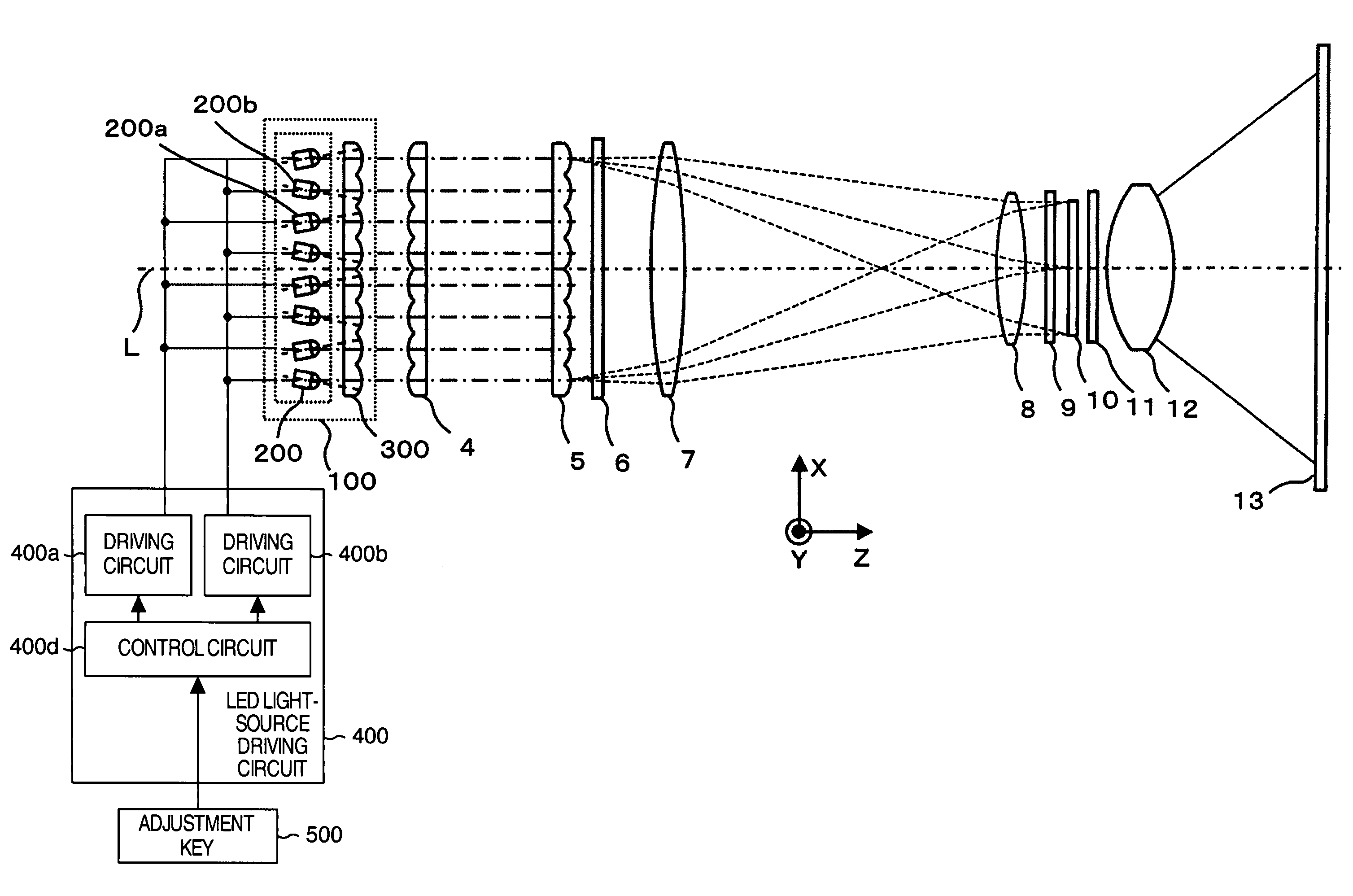
[0034]FIG. 1 is a schematic configuration diagram acquired by seeing from above an image display device which is a first embodiment according to the present invention.

[0035]In FIG. 1, a reference numeral 100 denotes a light-source unit. The light-source unit 100 is configured by a LED light source 200 including a plurality of LED elements for emitting monochromatic light, and a collimator lens (i.e., parallelizing unit) 300 for parallelizing the light from the LED light source 200. Numerals 4 and 5 respectively denote a first lens array and a second lens array which configure an integrator optical system. Numerals 6, 7, 8, 9, 10, 11, 12, and 13 denote a polarization conversion element, a light-converging lens, a condenser lens, an incoming-side sheet polarizer, a transparent-type liquid-crystal panel which is an image display element, an outgoing-side sheet polarizer, a projection lens, and a screen, respectively. A numeral 400 denotes a LED light-source driving ci...

second embodiment

[Second Embodiment]

[0076]In the first embodiment, with reference to the respective cell-lens optical axes of the collimator lens 300, the optical axes of the respective LED elements corresponding thereto are inclined. As a result, the lights on the optical axes outgoing from the light-emitting centers of the respective LED elements are caused to income into the rectangle-shaped configurations of the cell lenses of the first lens array 4 in such a manner that the lights have shifted (i.e., have deviated) from the centers of the rectangle-shaped configurations. This allows the lights on the optical axes of the respective LED elements to be illuminated onto the liquid-crystal panel and superimposed with each other thereon in such a manner that the lights are shifted from the central point of the liquid-crystal panel. This is because the light-source images from the respective LED elements formed on the cell lenses of the first lens array 4 are projected onto the liquid-crystal panel.

[0...

third embodiment

[Third Embodiment]

[0086]FIG. 10 is a schematic configuration diagram of an image display device which is a third embodiment according to the present invention. In FIG. 10, for each of LED panels designed for red, green, and blue lights, there is provided an illumination optical system whose configuration is the same as that of the illumination optical system in FIG. 1 for illuminating the light from the LED light-source unit onto the liquid-crystal panel.

[0087]In FIG. 10, numeral 100R denotes a red-oriented light-source unit, numeral 100G denotes a green-oriented light-source unit, and numeral 100B denotes a blue-oriented light-source unit.

[0088]The red-oriented light-source unit 100R is configured by a red-oriented LED light source 200R including a plurality of LED elements arranged in an array-like manner (m2 row×n2 column) and emitting red light, and a collimator lens 300R including a plurality of cell lenses which are similarly arranged in an array-like manner (m2 row×n2 column)...


PUM

PropertyMeasurementUnit
semiconductoraaaaaaaaaa
anglesaaaaaaaaaa
optical axesaaaaaaaaaa

Abstract

The image display device is configured to include the light source including a plurality of semiconductor light-emitting elements, a parallelizing unit including a plurality of cell lenses arranged in a one-to-one correspondence with each of the plurality of semiconductor light-emitting elements, an image display element for forming an optical image, a pair of lens-array groups located between the parallelizing unit and the image display element, and a projection unit for enlarging and projecting the optical image formed on the image display element. Moreover, the plurality of semiconductor light-emitting elements are located at substantially focal points of the cell lenses of the parallelizing unit. Furthermore, there exist at least two types of semiconductor light-emitting elements' groups, light beams on optical axes of the semiconductor light-emitting elements belonging to the two types of semiconductor light-emitting elements' groups existing on straight lines which are different from optical axes of the lens-array groups.

Description

INCORPORATION BY REFERENCE[0001]The present application claims priority from Japanese application JP2004-180438 filed on Jun. 18, 2004, the content of which is hereby incorporated by reference into this application.BACKGROUND OF THE INVENTION[0002]1. Field of the Invention[0003]The present invention relates to an image display device for illuminating an image display element, such as transparent-type liquid crystal, reflection-type liquid crystal, or DMD (micro mirror), by using light emitted from a light-source unit, and for enlarging and projecting an optical image formed on the image display element. Here, the light-source unit is configured by arranging a plurality of light sources such as LEDs which are semiconductor light-emitting elements.[0004]2. Description of the Related Art[0005]There has been known an image display device for illuminating an image display element, such as transparent-type liquid crystal, reflection-type liquid crystal, or DMD, by using light emitted from...

Claims


Application Information

Patent Timeline
Patent Type & Authority Patents(United States)
IPC IPC(8): G03B21/26F21V7/04G02B27/10G02F1/00G02F1/1335G03B21/20H01L33/00H04N5/74G02F1/13G03B21/00G03B21/14G03B37/04H04N9/31
CPCG03B37/04H04N5/7441H04N9/3105H04N9/3114H04N9/3141H04N9/3147H04N9/315H04N9/3197G03B21/2033Y10S362/80
Inventor YAMASAKI, FUTOSHIMASUOKA, NOBUOYATSU, MASAHIKO
Owner MAXELL HLDG LTD