Semiconductor chip and film and TAB package comprising the chip and film

a technology of semiconductor devices and tabs, which is applied in the direction of semiconductor devices, semiconductor/solid-state device details, electrical apparatus, etc., can solve the problems of reducing product performance and reliability, reducing routing space, etc., and achieve the effect of improving reliability

Active Publication Date: 2013-11-05
SAMSUNG ELECTRONICS CO LTD
View PDF19 Cites 6 Cited by
  • Summary
  • Abstract
  • Description
  • Claims
  • Application Information

AI Technical Summary

Benefits of technology

[0009]Example embodiments disclosed herein provide a semiconductor chip for a TAB package having improved reliability.
[0010]Example embodiments also provide a film for a TAB package having improved reliability.
[0011]Example embodiments additionally provide a TAB package having improved reliability.

Problems solved by technology

In pursuit of thinner, miniaturized devices, manufacturers may decrease the routing space (i.e., pitch) between lead wires and / or decrease the width of lead wires, both of which may decrease product performance and reliability.

Method used


Image

  • Semiconductor chip and film and TAB package comprising the chip and film
  • Semiconductor chip and film and TAB package comprising the chip and film
  • Semiconductor chip and film and TAB package comprising the chip and film

Examples


Embodiment Construction

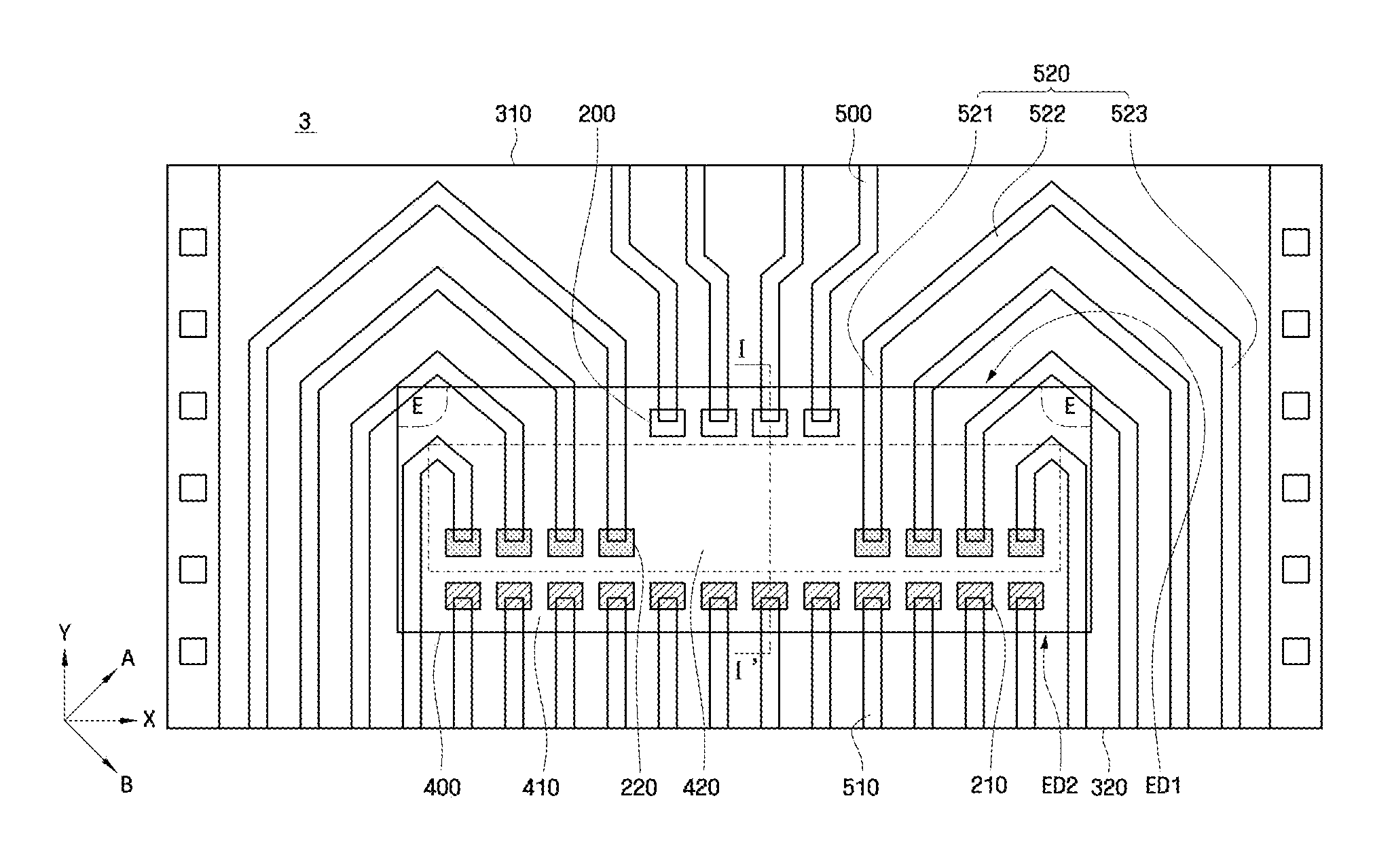
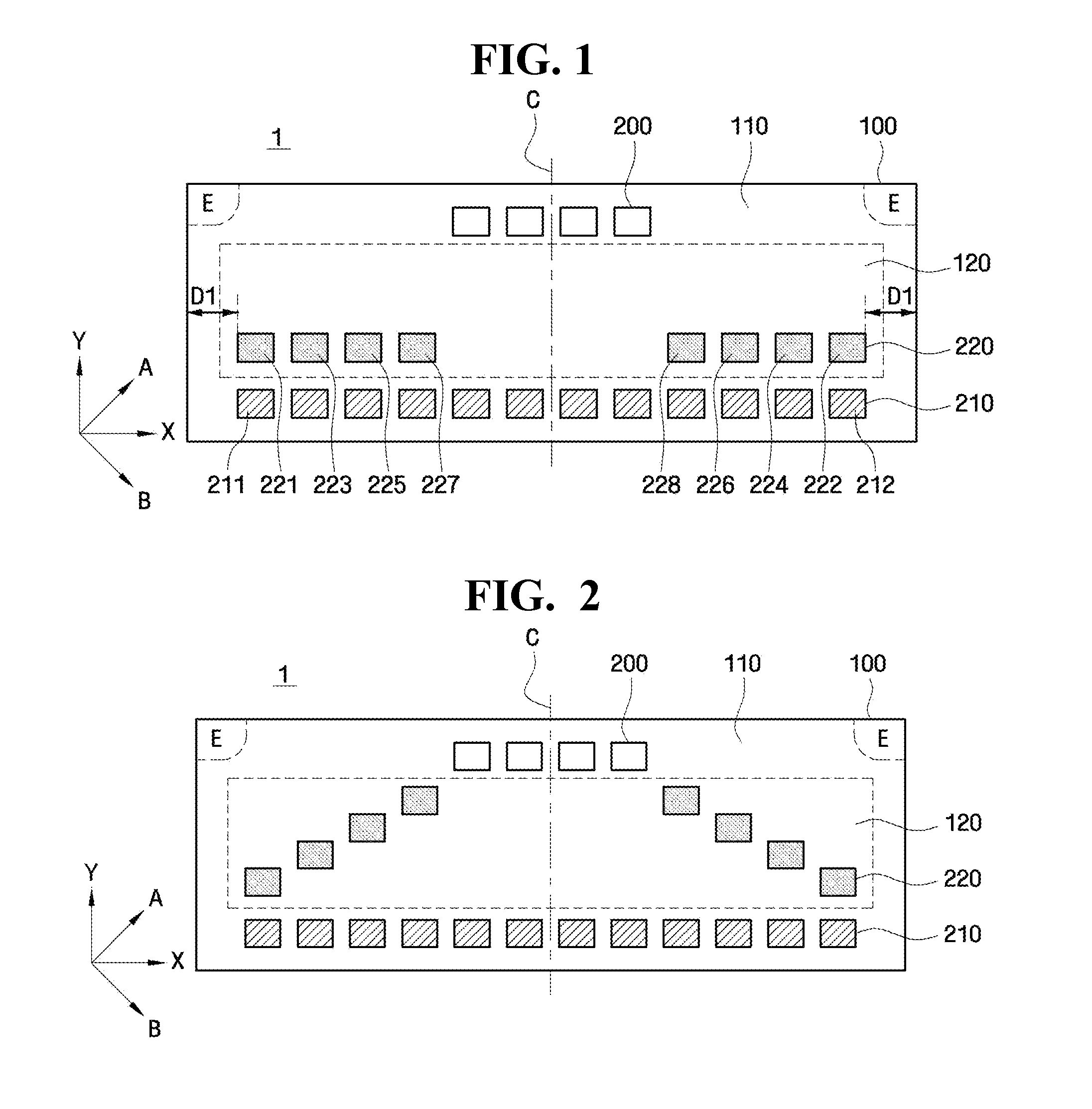
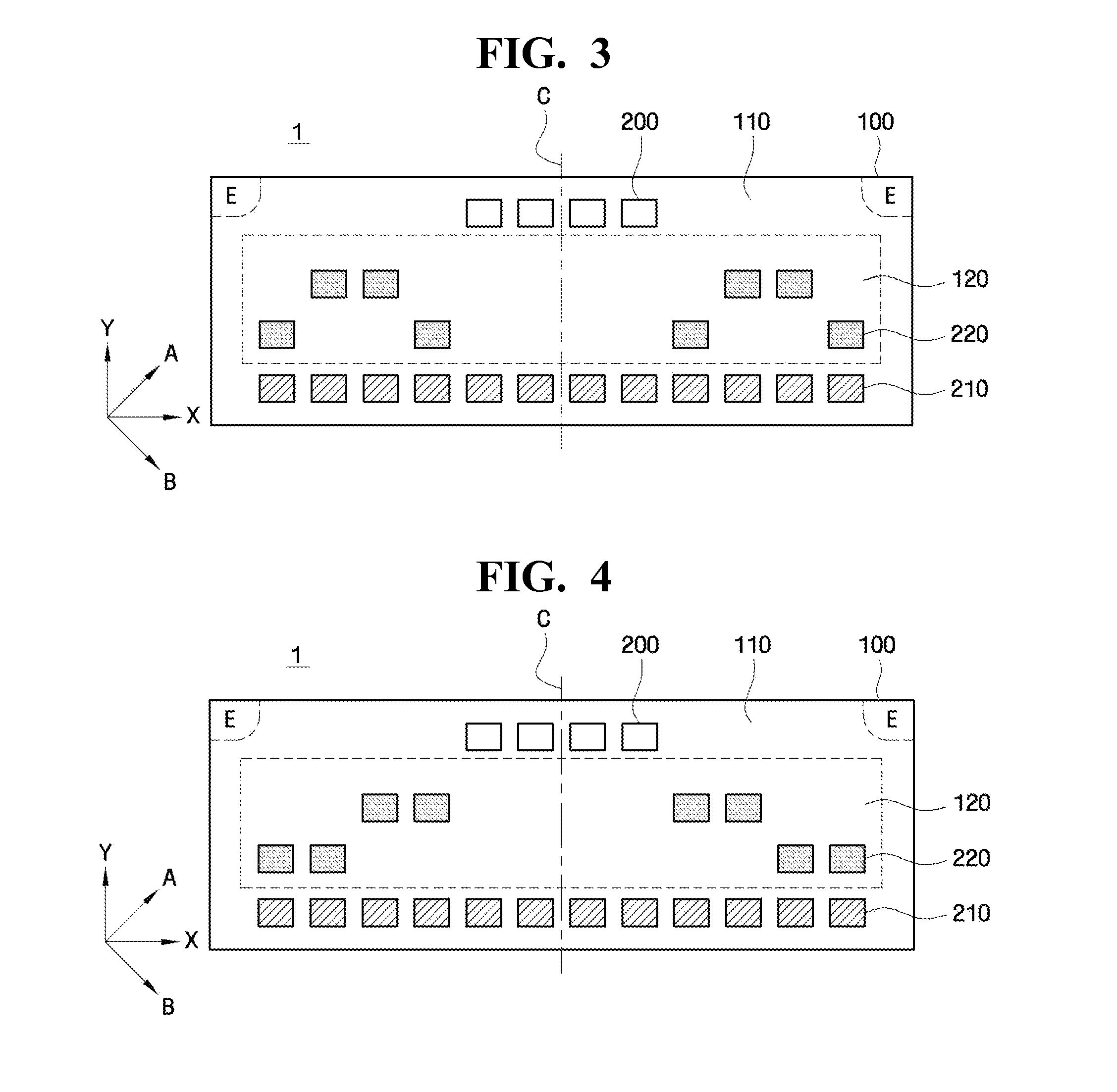
[0027]Advantages and features of the TAB package described herein and methods of manufacturing the same may be understood more readily by reference to the following detailed description of various exemplary embodiments and the accompanying drawings. The present invention may, however, be embodied in many different forms and should not be construed as being limited to the embodiments set forth herein. Rather, these embodiments are provided so that this disclosure will be thorough and complete and will fully convey the concepts disclosed herein to those skilled in the art, and the present invention will only be defined by the appended claims. In the drawings, the size and relative sizes of elements, layers, and regions may be exaggerated for clarity.

[0028]Like numbers refer to like elements throughout. As used herein, the term “and / or” includes any and all combinations of one or more of the associated listed items.

[0029]The terminology used herein is for the purpose of describing part...


PUM


Abstract

A semiconductor chip for a tape automated bonding (TAB) package is disclosed. The semiconductor chip comprises a connection surface including a set of input pads connected to internal circuitry of the chip and for conveying external signals to the internal circuitry, the set of input pads comprising all of the input pads on the chip. The connection surface includes a set of output pads connected to internal circuitry of the chip and for conveying internal chip signals to outside the chip, the set of output pads comprising all of the output pads on the chip.

Description

CROSS-REFERENCE TO RELATED APPLICATION[0001]This application claims priority under 35 U.S.C. 119 from Korean Patent Application No. 10-2010-0017747 filed on Feb. 26, 2010 in the Korean Intellectual Property Office, the contents of which in their entirety are herein incorporated by reference.BACKGROUND[0002]1. Field[0003]The disclosed embodiments relate to a semiconductor chip, a film, and a tape automated bonding (TAB) package comprising the chip and the film.[0004]2. Description of the Related Art[0005]There are numerous types of semiconductor packaging technologies. Specifically, TAB (Tape Automated Bonding) technology using an inner bead bonding (ILB) process has increasingly drawn attention.[0006]The TAB technique may provide a reel-to-reel package assembly using a reel type tape wiring board, and a package manufactured by the TAB technique is generally referred to as a TAB package. The TAB package may be classified into a chip on board (COB) and a tape carrier package (TCP).[00...

Claims


Application Information

Patent Timeline
Patent Type & Authority Patents(United States)
IPC IPC(8): H01L23/495
CPCH01L23/4985H01L24/50H01L24/06H01L2224/0401H01L2224/0405H01L2224/06155H01L2224/14155H01L2224/16227H01L2224/73204H01L2924/01029H01L2924/01078H01L2924/01079H01L2924/01082H01L2924/14H01L2924/01005H01L2924/01006H01L2924/01033H01L2924/01047H01L2924/0105H01L2224/16225H01L24/86H01L2224/05553
Inventor CHO, YOUNG-SANGKANG, CHANG-SIGSON, DAE-WOOCHOI, YUN-SEOKCHO, KYONG-SOONLEE, SANG-HEUL
Owner SAMSUNG ELECTRONICS CO LTD
Why Eureka
Try Eureka