Organic light emitting display device and manufacturing method for the same

a technology of light-emitting display and organic materials, which is applied in the direction of semiconductor devices, basic electric elements, electrical appliances, etc., can solve the problems of increased manufacturing cost, increased manufacturing cost, extended manufacturing time, etc., and achieves the effect of simplifying the manufacturing process

Inactive Publication Date: 2014-01-07
SAMSUNG DISPLAY CO LTD
View PDF18 Cites 6 Cited by
  • Summary
  • Abstract
  • Description
  • Claims
  • Application Information

AI Technical Summary

Benefits of technology

[0008]To solve the above and / or other problems, the present invention provides an organic light emitting display device having a simplified manufacturing process and satisfying all of a patterning characteristic, an electrical characteristic, and a pad reliability of a pad unit, and a method of manufacturing the organic light emitting display device.

Problems solved by technology

Accordingly, as the number of steps in which a mask is used increases, a manufacturing cost for preparing a mask increases.
Also, since the above-described complicated steps are needed, a manufacturing process is complicated, a manufacturing time is extended, and a manufacturing cost rises.

Method used


Image

  • Organic light emitting display device and manufacturing method for the same
  • Organic light emitting display device and manufacturing method for the same
  • Organic light emitting display device and manufacturing method for the same

Examples


Embodiment Construction

[0044]The attached drawings for illustrating exemplary embodiments of the present invention are referred to in order to gain a sufficient understanding of the present invention, the merits thereof, and the objectives accomplished by the implementation of the present invention. Hereinafter, the present invention will be described in detail by explaining exemplary embodiments of the invention with reference to the attached drawings. Like reference numerals in the drawings denote like elements.

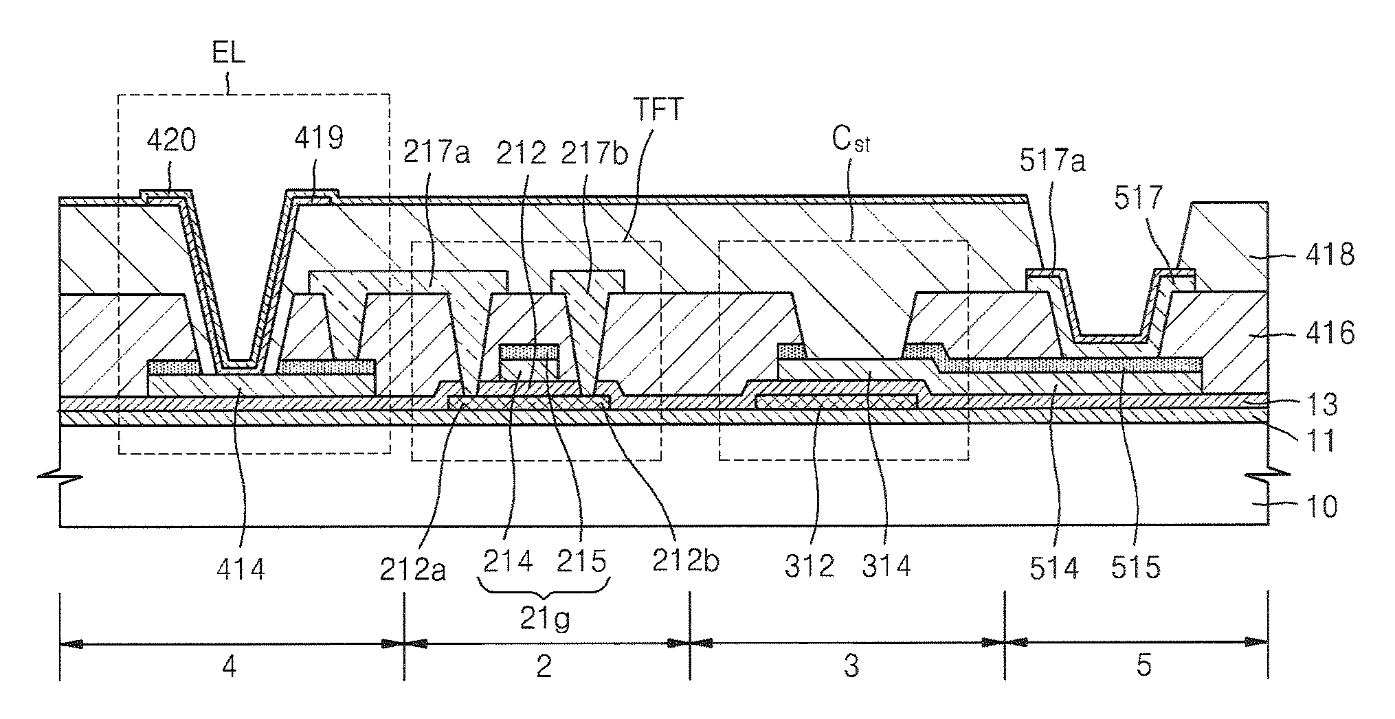
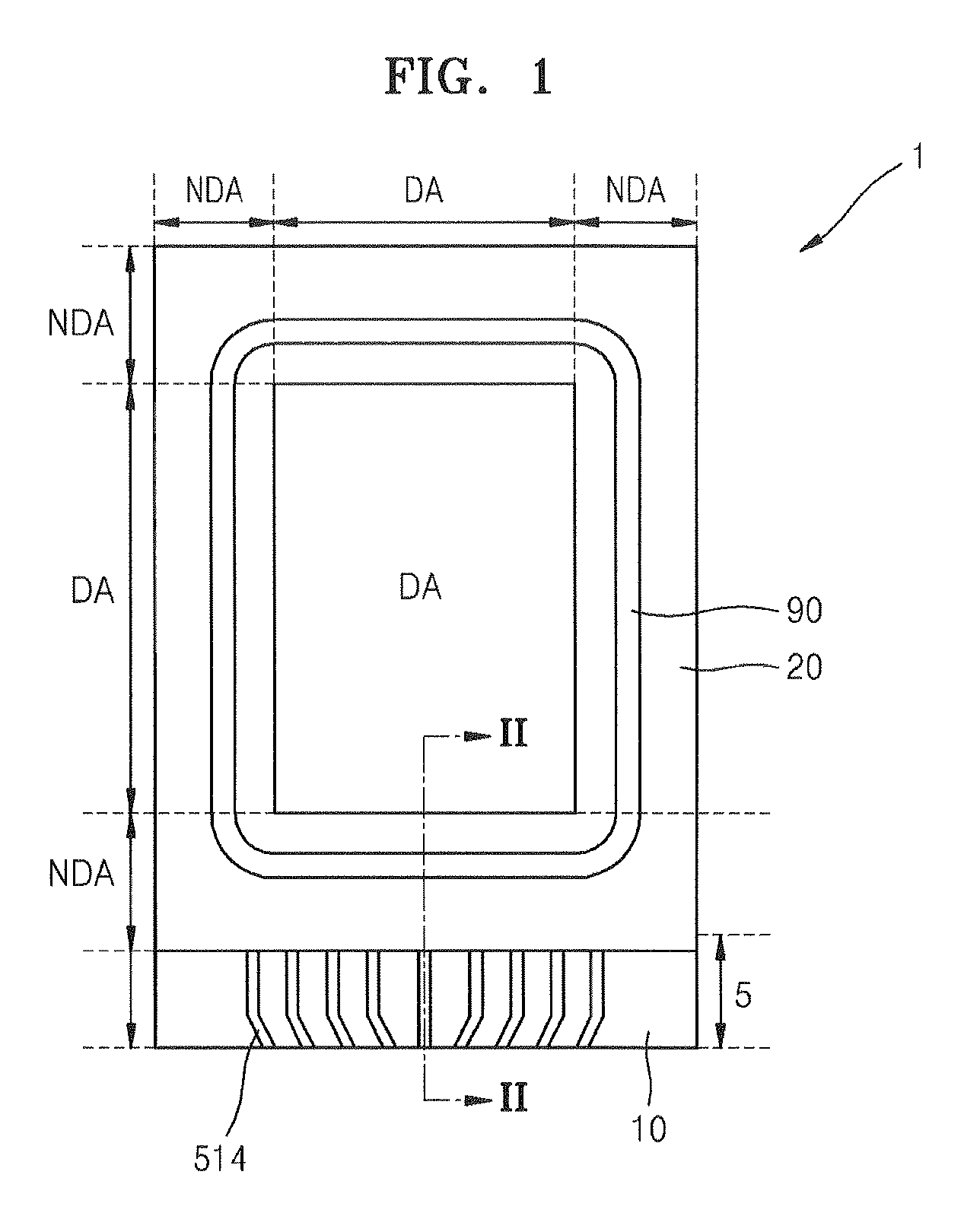
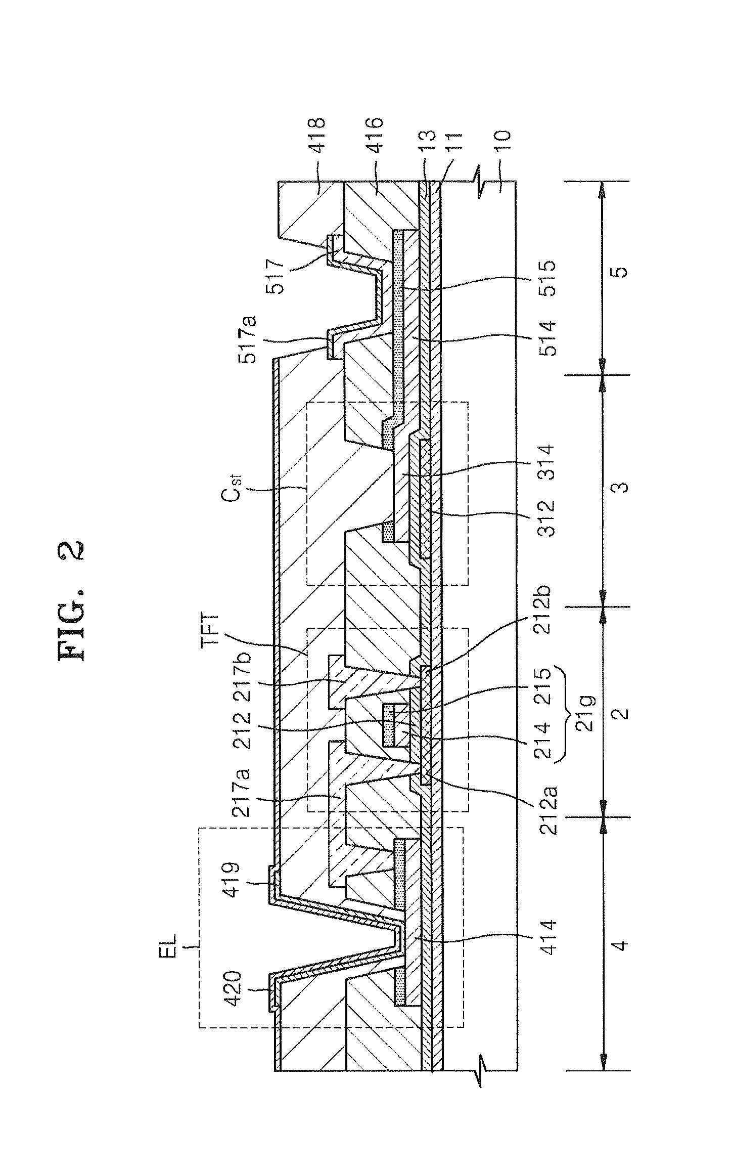
[0045]FIG. 1 is a plan view schematically illustrating the structure of an organic light emitting display device 1 according to an embodiment of the present invention. Referring to FIG. 1, the organic light emitting display device 1 according to the present embodiment includes a first substrate 10 including a thin film transistor (TFT) and a light emitting pixel, and a second substrate 20 that is coupled to the first substrate 10 via sealing.

[0046]The TFT, an organic electroluminescent device EL,...


PUM


Abstract

An organic light emitting display device includes a substrate, a thin film transistor formed on the substrate and including an active layer, a gate electrode including a gate lower electrode and a gate upper electrode, a source electrode, and a drain electrode, an organic light emitting device electrically connected to the thin film transistor, wherein a pixel electrode formed of the same material as at least a part of the gate electrode in the same layer, an intermediate layer including a light emitting layer, and an opposed electrode arranged to face the pixel electrode are sequentially deposited.

Description

CLAIM OF PRIORITY[0001]This application makes reference to, incorporates the same herein, and claims all benefits accruing under 35 U.S.C. §119 from an application earlier filed in the Korean Intellectual Property Office on 8 Dec. 2010 and there duly assigned Serial No. 10-2010-0124863.BACKGROUND OF THE INVENTION[0002]1. Field of the Invention[0003]The present invention relates to an organic light emitting display device and a manufacturing method thereof, and more particularly, to an organic light emitting display device having a simplified manufacturing process and satisfying all of a patterning characteristic, an electrical characteristic, and a pad reliability of a pad unit, and a method of manufacturing the organic light emitting display device.[0004]2. Description of the Related Art[0005]Flat panel display devices such as organic light emitting display devices or liquid crystal display devices are manufactured on a substrate on which a pattern including thin film transistors (...

Claims


Application Information

Patent Timeline
Patent Type & Authority Patents(United States)
IPC IPC(8): H01L29/16H01L29/04H01L29/15H01L29/18
CPCH01L27/3276H01L2227/323H01L27/3248H01L29/18H01L51/56H01L27/14H01L21/00H10K59/123H10K59/131H10K59/1201H10K71/00
Inventor LEE, JUNE-WOOYOU, CHUN-GICHOI, JOON-HOO
Owner SAMSUNG DISPLAY CO LTD
Why Eureka
Try Eureka