

Antenna device and wireless communication device
a wireless communication and antenna device technology, applied in loop antennas with ferromagnetic cores, instruments, sensing by electromagnetic radiation, etc., can solve the problems of narrowing the required communication band width and general decrease of antenna device radiation capabilities, and achieve the effect of increasing the size of the devi
- Summary
- Abstract
- Description
- Claims
- Application Information
AI Technical Summary
Benefits of technology
Problems solved by technology
Method used
Image

Examples
first preferred embodiment
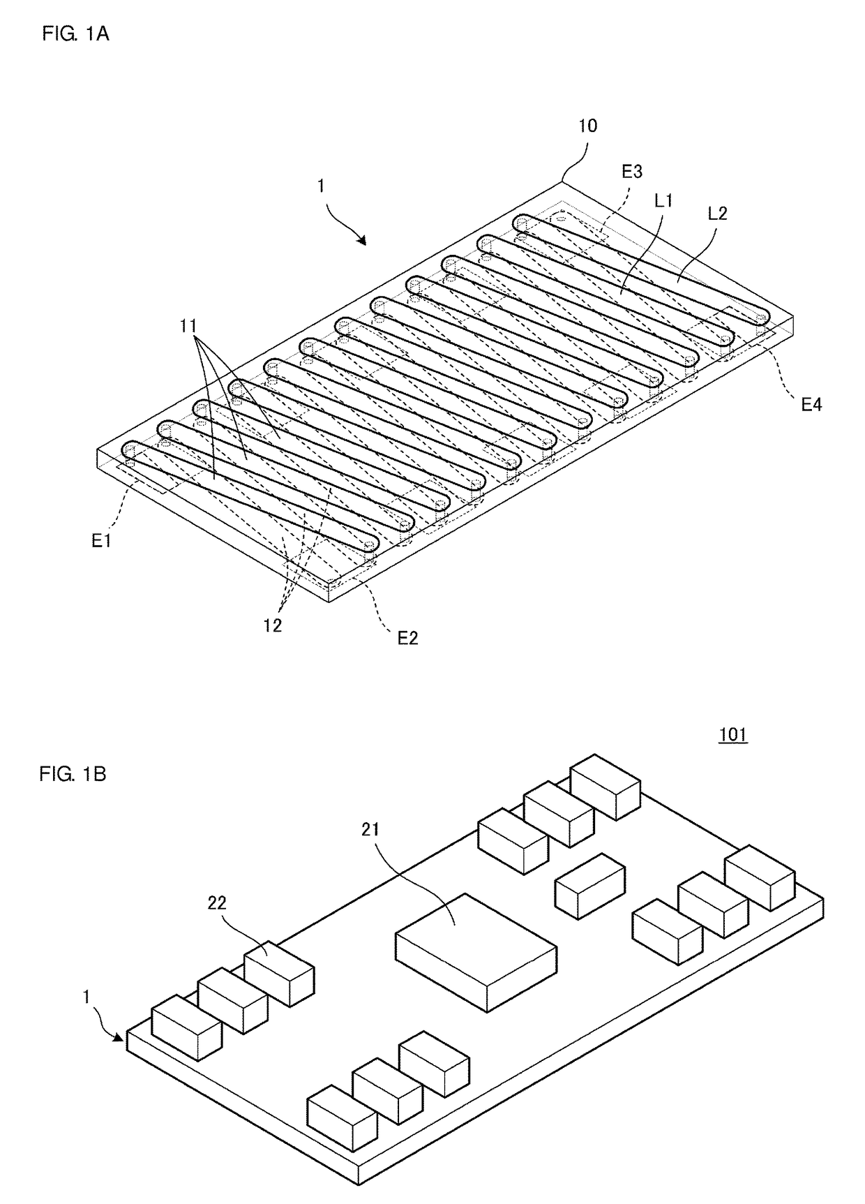
[0039]FIG. 1A is a perspective view illustrating a coil antenna 1 that is one constituent element in an antenna device according to a first preferred embodiment of the present invention. FIG. 1B is a perspective view illustrating an antenna device 101 formed by mounting a plurality of chip components on an upper area of the coil antenna 1.
[0040]The coil antenna 1 illustrated in FIG. 1A is constituted by a multilayer body 10 preferably formed by laminating a plurality of insulators in which conductor patterns are formed. FIGS. 1A and 1B depict the interior of the multilayer body in a transparent manner.
[0041]An upper conductor pattern 11, a lower conductor pattern 12, and an interlayer connecting conductor that defines an interlayer connection between the upper conductor pattern 11 and the lower conductor pattern 12 are provided in the multilayer body 10, thus defining a first coil L1 and a second coil L2 that each include a plurality of turns.
[0042]The first coil and the second coil...
second preferred embodiment
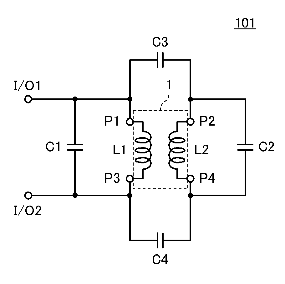
[0068]FIG. 8 is an equivalent circuit diagram illustrating an antenna device 102 according to a second preferred embodiment of the present invention. The configurations of the coil antenna 1 and the capacitances C1, C2, C3, and C4 are the same as those described in the first preferred embodiment and illustrated in FIG. 6B. In the present preferred embodiment, first power supply terminals Output1 and Output2 are connected to the first resonance circuit defined by the parallel circuit of the first coil L1 and the first capacitance C1. Meanwhile, second power supply terminals Input1 and Input2 are connected to the second resonance circuit defined by the parallel circuit of the second coil L2 and the second capacitance C2.
[0069]In FIG. 8, impedance frequency characteristics of the antenna device as viewed from the first power supply terminals Output1 and Output2 differ from impedance frequency characteristics of the antenna device as viewed from the second power supply terminals Input1 ...
third preferred embodiment
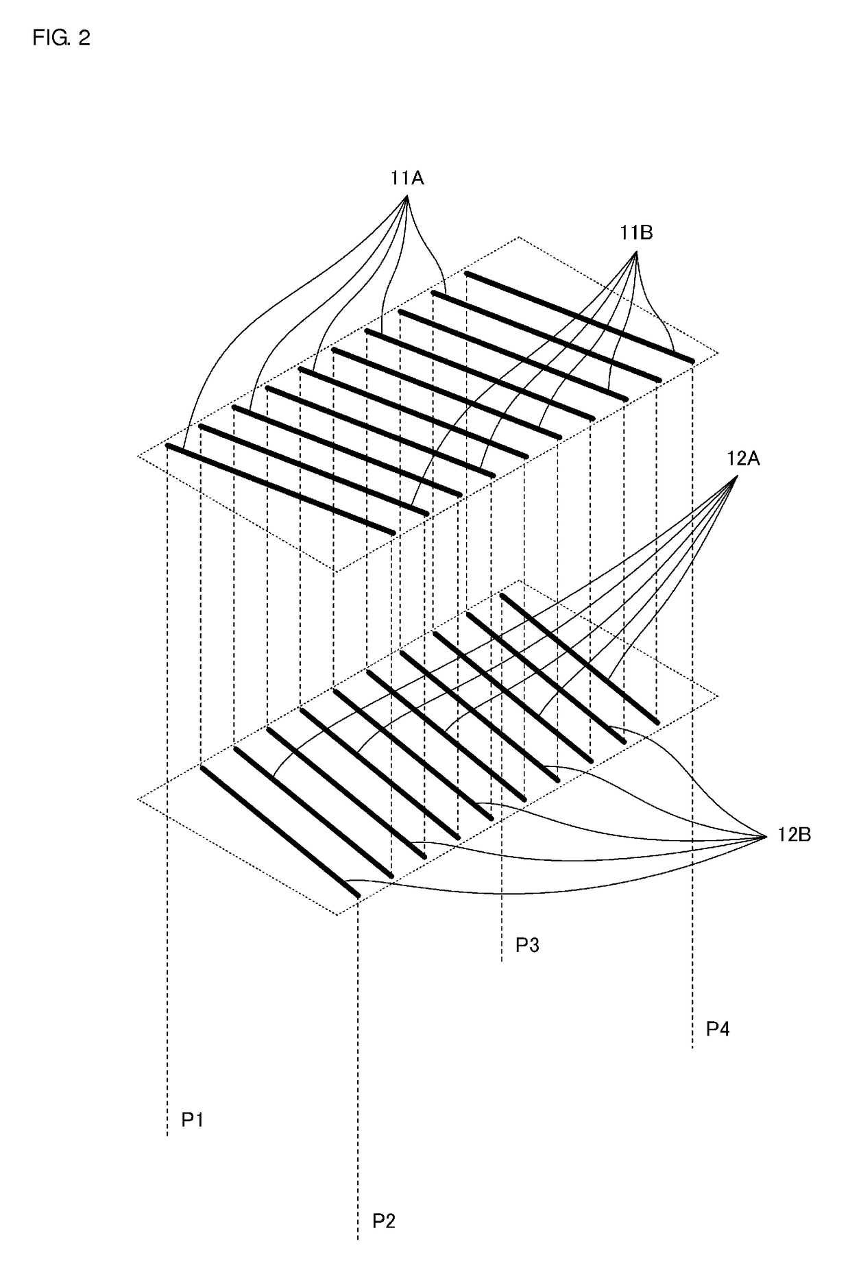
[0080]FIG. 10 is a perspective view illustrating the configuration of a coil antenna included in an antenna device according to a third preferred embodiment of the present invention. The overall shapes of the first coil and the second coil are illustrated here in particular. The upper conductor patterns 11A and 11B are provided on a predetermined upper base material layer and the lower conductor patterns 12A and 12B are provided on a predetermined lower base material layer. Furthermore, an interlayer connecting conductor that connects the upper conductor pattern 11A and the lower conductor pattern 12A is provided, and the first coil is defined by this interlayer connecting conductor, the upper conductor pattern 11A, and the lower conductor pattern 12A. Likewise, an interlayer connecting conductor that connects the upper conductor pattern 11B and the lower conductor pattern 12B is provided, and the second coil is formed by this interlayer connecting conductor, the upper conductor pat...
PUM
 Abstract
Description
Claims
Application Information