
Method and arrangement for manufacturing optical products with complex three-dimensional forms
A three-dimensional shape, complex technology, applied in the direction of semiconductor/solid-state device manufacturing, electrical components, circuits, etc., can solve problems such as unsolved, achieve the effect of easy construction and reduced duration
Patent Information
- Authority / Receiving Office
- CN · China
- Patent Type
- Applications(China)
- Current Assignee / Owner
- Publication Date
- 2009-12-02
Smart Images
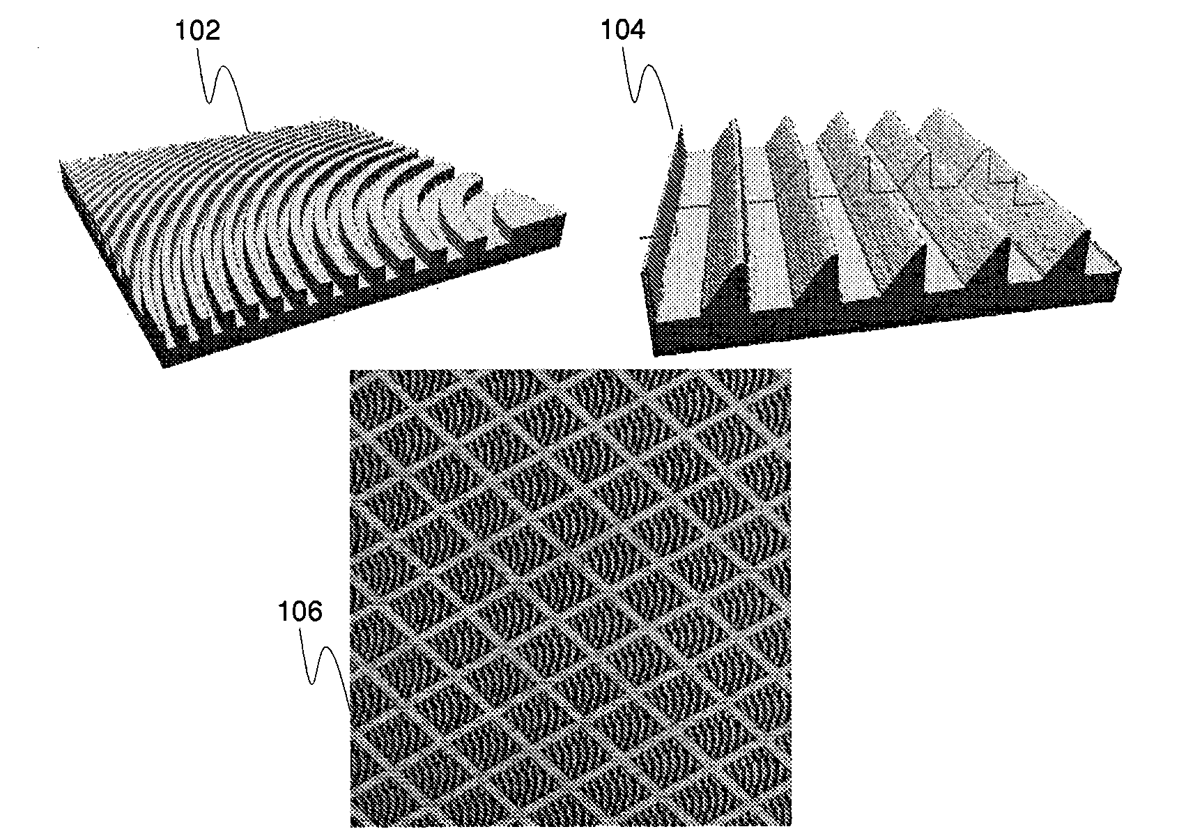
Figure 1 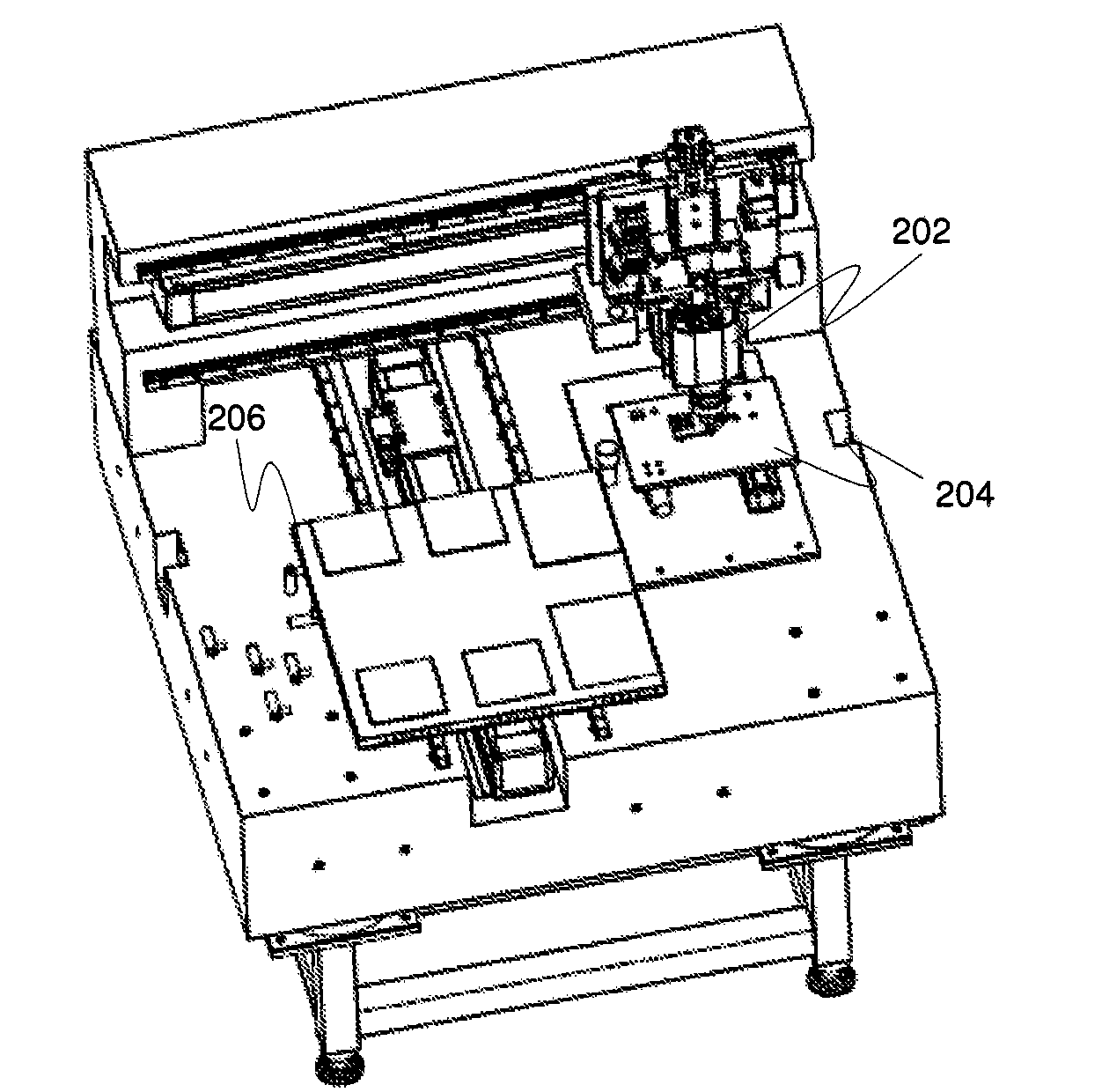
Figure 2 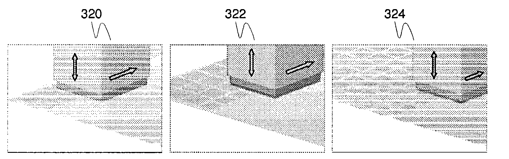
Figure 3
Abstract
Description
technical field
[0001] In general, the present invention relates to optics and optoelectronics. In particular, the invention relates to methods of fabricating optical microstructures. Background technique
[0002] There is an increasing need to improve light management and luminous efficiency in many lighting applications. This premise applies in particular to LED (Light Emitting Diode) lighting. To achieve the desired lighting performance, efficient optics with point light sources such as LEDs need to be used. Solutions utilizing diffractive optics or other complex micro-optical structures offer a host of new possibilities for advanced illumination including dimensional benefit and cost-effective integration.
[0003] Typically, the fabrication of diffractive (DO) or other micro-optical structures is done by photolithographic processes such as mask lithography, direct laser beam or electron beam writing. These methods have certain disadvantages which greatly limit the f...
Examples
Embodiment Construction
[0055] The advanced step embossing method according to the present invention typically utilizes multiple different embossing tools to produce variable micro-optical (eg DO) patterns with eg binary and / or blazed grating profiles. This profile is in the form of a surface relief pattern on the substrate. The substrate here is the material on which the micro-optical pattern is actually formed, and the substrate itself may be placed on top of a different carrier medium, eg as an uppermost layer. The imprint tool can be manufactured by high-precision micromachining or photolithography according to the required micro-optical structure. In addition, a novel imprint tool manufacturing method will be proposed hereinafter. Micromachining is more suitable for inclined structures such as 45° blazed gratings than photolithographic methods, however, photolithography is feasible for eg binary grooves. In microfabrication, generally, it is advantageous to focus on high-quality structures tha...