
Wave control architecture integrating work and test simulation and wave control method
An integrated and working technology, applied in the direction of program control, computer control, general control system, etc., to achieve the effect of improving testability and maintainability, improving efficiency and reducing verification time
Patent Information
- Authority / Receiving Office
- CN · China
- Patent Type
- Patents(China)
- Current Assignee / Owner
- Publication Date
- 2014-08-20
Smart Images
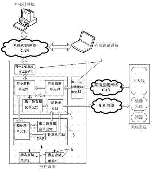
Figure 1 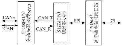
Figure 2 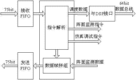
Figure 3
Abstract
Description
technical field
[0001] The invention relates to the field of radar wave control design, in particular to a wave control structure and a wave control method integrating work and test simulation. Background technique
[0002] With the continuous increase of the radar scale, the complexity of the wave control system is also increasing, and more and more special situations are encountered in the research and development process. When the traditional wave control system fails, it needs to run the simulation debugging program to find the fault. The testability and maintainability of the system are not high; and the simulation debugging program of the FPGA module and the simulation debugging program of the DSP module need to be run separately. Performing two calculation verifications increases the verification time of the system and reduces the work efficiency. The wave control architecture that integrates testing and simulation can solve the above problems well. Contents of the...
Examples
Embodiment
[0020] A wave control architecture integrating work and test simulation, the architecture includes CAN bus interface module 1, FPGA module 2, DSP module 3, CAN bus interface module includes a first CAN bus interface unit 11 and includes a second CAN bus interface Unit 12; FPGA module 2 mainly includes instruction analysis unit 21, number sending unit 22, front monitoring unit 23 and first simulation debugging unit 24; DSP module 3 mainly includes preprocessing unit 31, second simulation debugging unit 32 and calculation unit 33 ; the storage module 4 mainly includes a dynamic storage unit 41 and a static storage unit 42 .
[0021] The simulation debugging unit is divided into two parts, which are respectively located in the FPGA module 2 and the DSP module 3, both of which can receive debugging instructions and work together. The part in the FPGA module 2 is the first simulation debugging unit 24, which can simulate and generate system signals such as the start signal (ST), th...