
Etching method for silicon nitride high depth-to-width ratio hole
A high aspect ratio, silicon nitride technology, used in electrical components, circuits, semiconductor/solid-state device manufacturing, etc., can solve problems such as low selectivity ratio, etching suspension, and difficulty in obtaining etching topography
Patent Information
- Authority / Receiving Office
- CN · China
- Patent Type
- Applications(China)
- Current Assignee / Owner
- Publication Date
- 2014-01-22
Smart Images
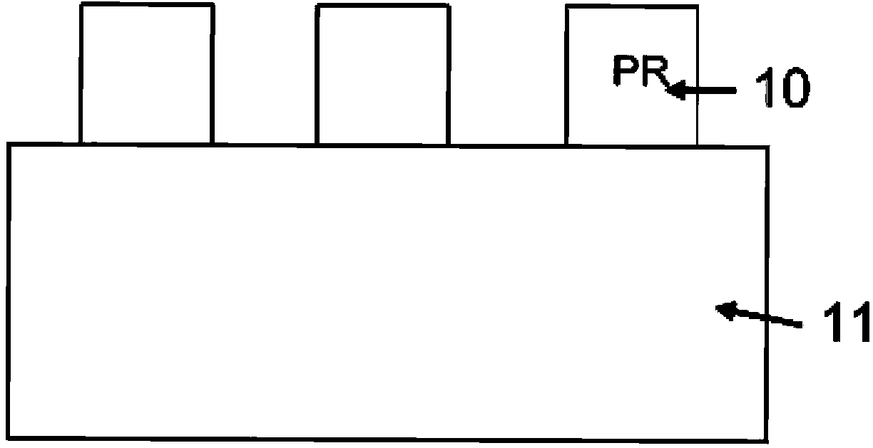
Figure 1 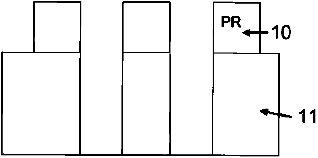
Figure 2 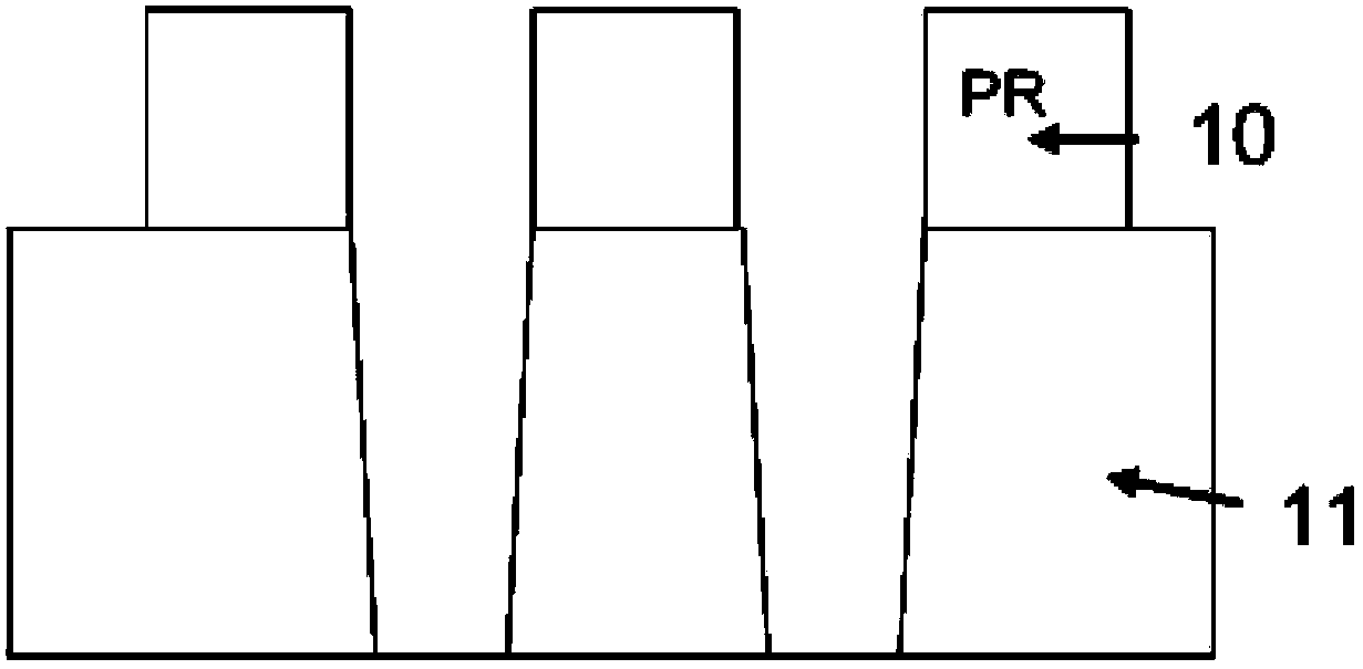
Figure 3
Abstract
Description
technical field
[0001] The invention belongs to the field of semiconductor integrated circuit manufacturing, and more specifically relates to an etching method for a silicon nitride film with a high aspect ratio hole. Background technique
[0002] Contact hole etching is a key technology of VLSI. As CMOS enters the technology era after 32nm, high aspect ratio hole etching and its filling have a considerable impact on the yield of devices. For advanced memories, the aspect ratio has reached more than 40:1, which makes the challenge even greater.
[0003] The contact hole etching medium of traditional CMOS devices is silicon dioxide film. As another widely used dielectric material, silicon nitride is hardly used as an ILD layer due to its large K value and stress. It is mainly used as a stop layer for hard mask, etch or CMP.
[0004] Similar to the etching of silicon oxide films, for silicon nitride films, fluorocarbon-based gases such as CF 4 、CHF 3 、CH 2 f 2 、CH 3 F e...
Examples
Embodiment Construction
[0023] The present invention will be described in detail below in conjunction with the accompanying drawings and by taking specific implementations as examples. However, those skilled in the art should know that the present invention is not limited to the specific embodiments listed, as long as it conforms to the spirit of the present invention, it should be included in the protection scope of the present invention.
[0024] The etching method of the silicon nitride high aspect ratio hole of the present invention comprises the following steps:
[0025] First, put the silicon nitride film structure wafer with the required pattern developed by photolithography into the etching chamber; Inert gas, hydrogen-containing fluorocarbon-based gas, and radio frequency power are added to excite the plasma; after the plasma stabilization step, the silicon nitride film is etched until the etching morphology and aperture size of the high aspect ratio hole and The depth meets the requirement...