
Multi-channel dvi image fusion correction control host
A technology of correction control and image fusion, applied in instruments, electrical digital data processing, digital output to display devices, etc., can solve the problem that the synchronization and real-time performance of multi-channel display output content cannot be completely consistent, the hardware performance requirements are high, and the cost of GPU graphics cards is high. problem, to achieve the effect of good image fusion, improved refresh synchronization, and high correction quality.
Patent Information
- Authority / Receiving Office
- CN · China
- Patent Type
- Patents(China)
- Current Assignee / Owner
- Publication Date
- 2017-08-01
Smart Images
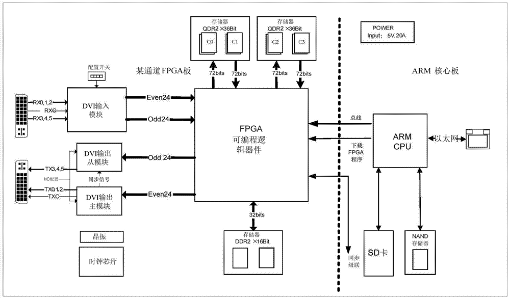
Figure 1 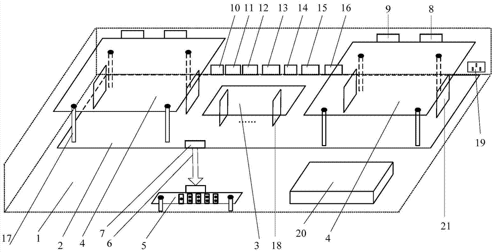
Figure 2 
Figure 3
Abstract
Description
[0001] 1. Technical field
[0002] The invention belongs to the technical field of electronic applications and relates to multi-channel image fusion technology, in particular to a multi-channel DVI image fusion correction control host.
[0003] 2. Background technology
[0004] At present, in response to the demand for large-scale projection display and LED screen display, there are more and more application occasions for merging multiple display channel images into one large-scale scene image output. It is mainly aimed at high-resolution, large field of view, and special-shaped curved surface projection environments. It is used in training centers, command and control centers, large-scale conference display screens, data display environments in financial centers, visualization of manufacturing control, and visualization environments of urban management.
[0005] The structural solution widely used in large-scale display systems is the high-performance PC networking synchroniza...
Examples
Embodiment Construction
[0031] Accompanying drawing has provided a specific embodiment.
[0032] The various components of the calibration control host are installed in the chassis, which is a standard 3U chassis with air cooling, conduction and other heat dissipation methods. The length × width × height is about 4250 × 4350 × 1320 (mm), and the chassis shell has 4 mounting holes and grounding stakes. The casing is made of metal casing and aluminum profile.
[0033] There are motherboard, ARM core board, FPGA channel board and light board in the chassis. The various components are laid out on the respective boards. The ARM CPU module is set on the ARM core board, and the FPGA programmable logic device, DVI input module, DVI output module, QDR2 data access module, and DDR2 data access module are set on the FPGA board. The DVI input module is installed on the DVI output port 8 of the FPGA channel board, and the DVI output module is installed on the DVI input port 9 of the FPGA channel board. It is ...