
Semiconductor device structure and fabrication method thereof
A device structure and semiconductor technology, applied in the fields of semiconductor devices, semiconductor/solid-state device manufacturing, electrical components, etc., can solve the problems of low yield of critical size chips, etc.
Patent Information
- Authority / Receiving Office
- CN · China
- Patent Type
- Patents(China)
- Current Assignee / Owner
- Publication Date
- 2019-03-22
Smart Images
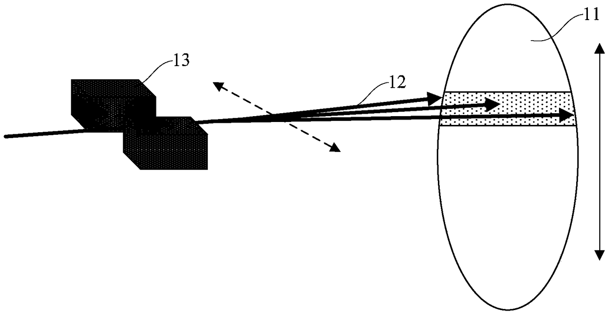
Figure 1 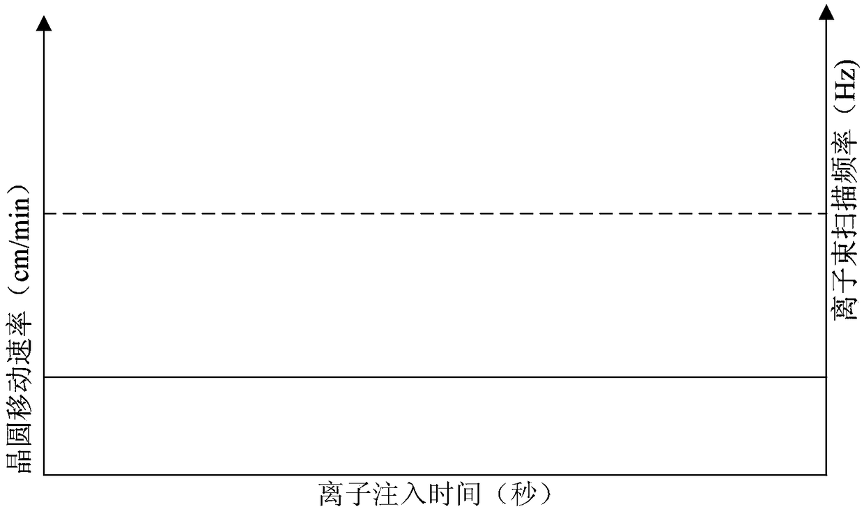
Figure 2 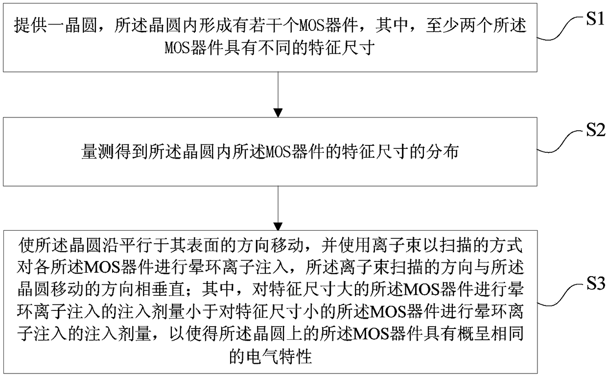
Figure 3
Abstract
Description
technical field
[0001] The invention belongs to the technical field of semiconductor manufacturing, and in particular relates to a semiconductor device structure and a preparation method thereof. Background technique
[0002] The metal oxide semiconductor field effect transistor (MOSFET) structure is widely used in the manufacturing process of semiconductor integrated circuits (IC). The electrical characteristics of MOSFET devices are related to the thickness of the gate oxide layer (GOX THK) and the distance between source and drain. (Critical dimension, that is, the gate width of the MOSFET device, that is, the channel length between the source and drain regions in the MOSFET device) is closely related to the ion implantation process.
[0003] In order to reduce the channel effect of the device, halo ion implantation (Haloimplant) is generally performed on the MOSFET device at present, so as to form a ring-shaped halo implantation region in the channel of the MOSFET device...
Examples
Embodiment 1
[0062] see figure 1 , the invention provides a kind of preparation method of semiconductor device structure, the preparation method of described semiconductor device structure comprises the following steps:
[0063] 1) providing a wafer in which several MOS devices are formed, wherein at least two of the MOS devices have different feature sizes;
[0064] 2) measuring and obtaining the distribution of the characteristic sizes of the MOS devices in the wafer;
[0065] 3) moving the wafer in a direction parallel to its surface, and performing halo ion implantation on each of the MOS devices in a scanning manner using an ion beam, the scanning direction of the ion beam is the same as the moving direction of the wafer The directions are perpendicular; wherein, the implantation dose of halo ion implantation for the MOS device with a large feature size is smaller than the implantation dose for halo ion implantation for the MOS device with a small feature size, so that the The MOS d...
Embodiment 2
[0091] Please continue to refer to Embodiment 1 Figure 4 to Figure 15 , the present invention also provides a semiconductor device structure, the semiconductor device structure is prepared by the preparation method described in Embodiment 1, the semiconductor device structure includes: a number of MOS devices arranged at intervals, wherein at least two Each of the MOS devices has different feature sizes; an annular halo implantation region 25 is formed in the channel of each of the MOS devices, and the ion implantation concentration in the halo implantation region 25 is inversely proportional to that of the MOS device. Feature size.
[0092] As an example, the ion implantation concentration in the halo implantation region 25 in the MOS device with a relatively large feature size is lower than the ion implantation concentration in the halo implantation region 25 in the MOS device with a small relative feature size, , to ensure that the MOS devices on the wafer 21 have substan...