
Two-dimensional magnetically driven scanning micromirror based on mems technology and its preparation method
A technology of scanning micromirror and technology, which is applied to the technology for producing decorative surface effects, metal material coating technology, microstructure devices composed of deformable elements, etc., can solve the difficulty of integrating micro-actuating devices, sensors and There are huge differences in the working principle and structural scheme of the driver, and there is no process standard for MEMS devices, etc.
Patent Information
- Authority / Receiving Office
- CN · China
- Patent Type
- Patents(China)
- Current Assignee / Owner
- Publication Date
- 2020-07-07
Smart Images
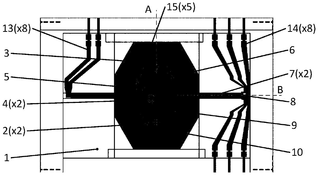
Figure 1 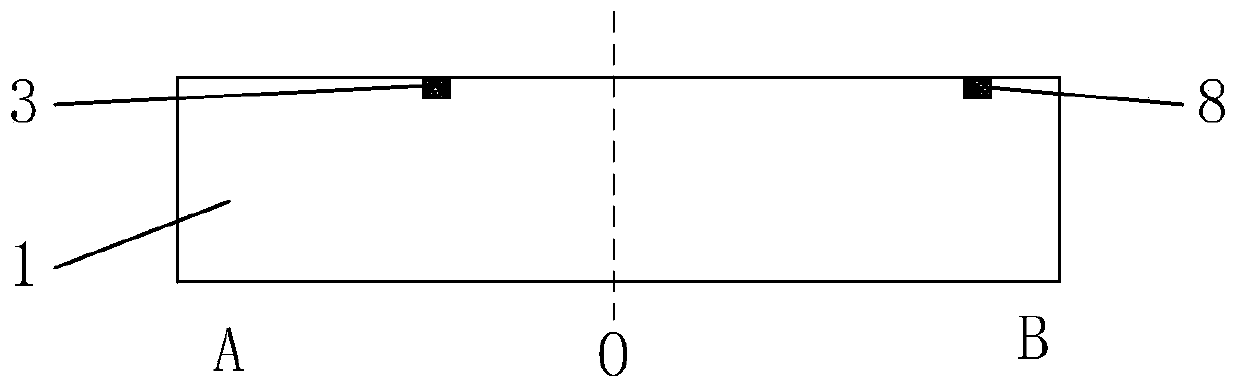
Figure 2 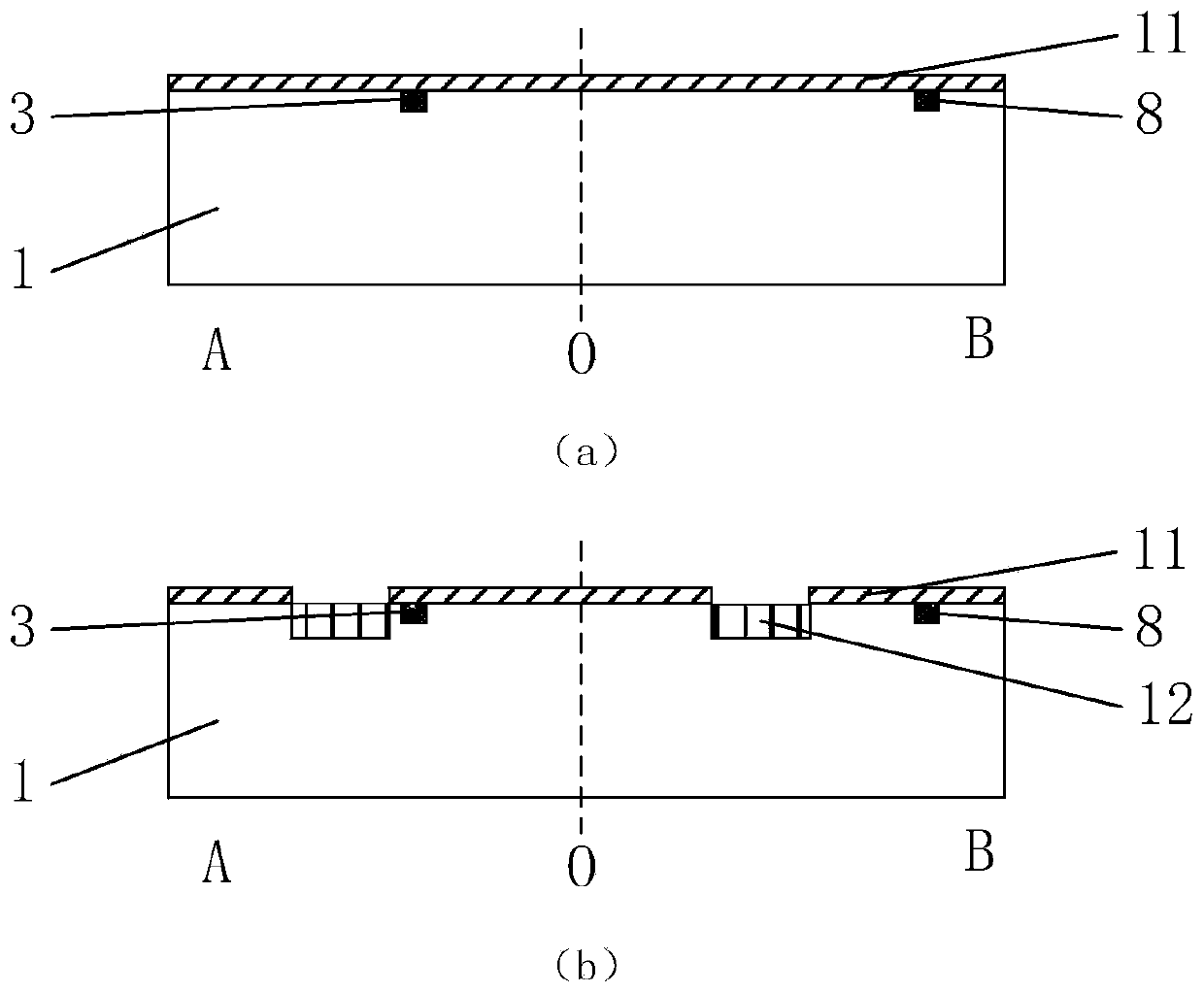
Figure 3
Abstract
Description
technical field
[0001] The invention belongs to the technical field of microelectromechanical systems, in particular to a two-dimensional magnetically driven scanning micromirror based on MEMS technology and a preparation method thereof. Background technique
[0002] With the advancement of micromachining technology and the application requirements of miniaturized sensor and actuator systems, the two-dimensional magnetically driven scanning micromirror based on MEMS technology is used as a micro-actuating device in LiDAR imaging systems. Its function is to obtain three-dimensional space information by changing the rotation angle of the mirror, changing the exit angle of the laser beam, receiving and processing after being reflected by the object. Compared with traditional mechanical radars, MEMS micromirrors generally require a surface size of more than 1mm, and the overall size is small, easy to drive, and has the possibility of embedded assembly.
[0003] Compared with in...
Examples
preparation example Construction
[0038] A kind of preparation method of the two-dimensional magnetic drive scanning micromirror based on MEMS technology of the present invention, comprises the following steps:
[0039] Step 1, preparing the first piezoresistive sensor 3 and the second piezoresistive sensor 8 on the silicon substrate 1;
[0040] 1.1. Photolithography forms the graphics of the first piezoresistive sensor 3 and the second piezoresistive sensor 8:
[0041] Coating positive photoresist on the silicon substrate 1, covering the mask plate provided with the patterns of the first piezoresistive sensor 3 and the second piezoresistive sensor 8, and performing exposure treatment to obtain the first piezoresistive sensor 3 and the second piezoresistive sensor The graph of resistance sensor 8.
[0042] 1.2. Perform reactive ion etching on the silicon substrate 1 to obtain the structures of the first piezoresistive sensor 3 and the second piezoresistive sensor 8, and obtain an alignment mark structure;
...
Embodiment
[0084] combine Figure 1 to Figure 7 , a two-dimensional magnetically driven scanning micromirror based on MEMS technology of the present invention, comprising a silicon substrate 1, a mirror substrate 6, a first piezoresistive sensor 3, a second piezoresistive sensor 8, a coil 9, a frame 10, an oxide insulating layer 4. Metal mirror layer 5, metal electrodes 14, coil leads 13, metal connecting wires, two first cantilever beams 2 and two second cantilever beams 7 arranged symmetrically to the center of the mirror base 6, and the two first cantilever beams 2 is perpendicular to the line connecting the two second cantilever beams 7;
[0085] The specific preparation process includes the following steps:
[0086] Step 1, preparing the first piezoresistive sensor 3 and the second piezoresistive sensor 8; as figure 2 shown;
[0087] 1.1. Photolithography forms the graphics of the first piezoresistive sensor 3 and the second piezoresistive sensor 8:
[0088] Coating AZ5214 posi...