
Lateral diffused metal oxide semiconductor field effect transistor
A technology of oxide semiconductors and field effect transistors, which is applied in the field of laterally diffused metal oxide semiconductor field effect transistors, can solve problems such as burning integrated circuits, gate damage, and component damage, so as to reduce resistance, increase component area, and improve The effect of breakdown voltage and high temperature reverse bias test
Patent Information
- Authority / Receiving Office
- CN · China
- Patent Type
- Applications(China)
- Current Assignee / Owner
- Publication Date
- 2019-04-09
Smart Images
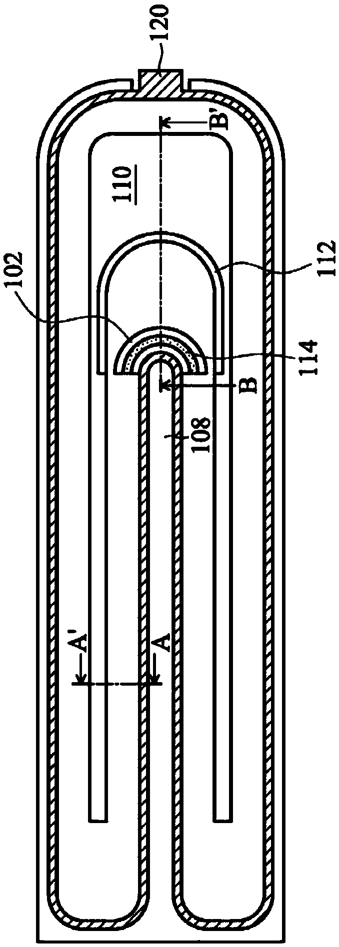
Figure 1 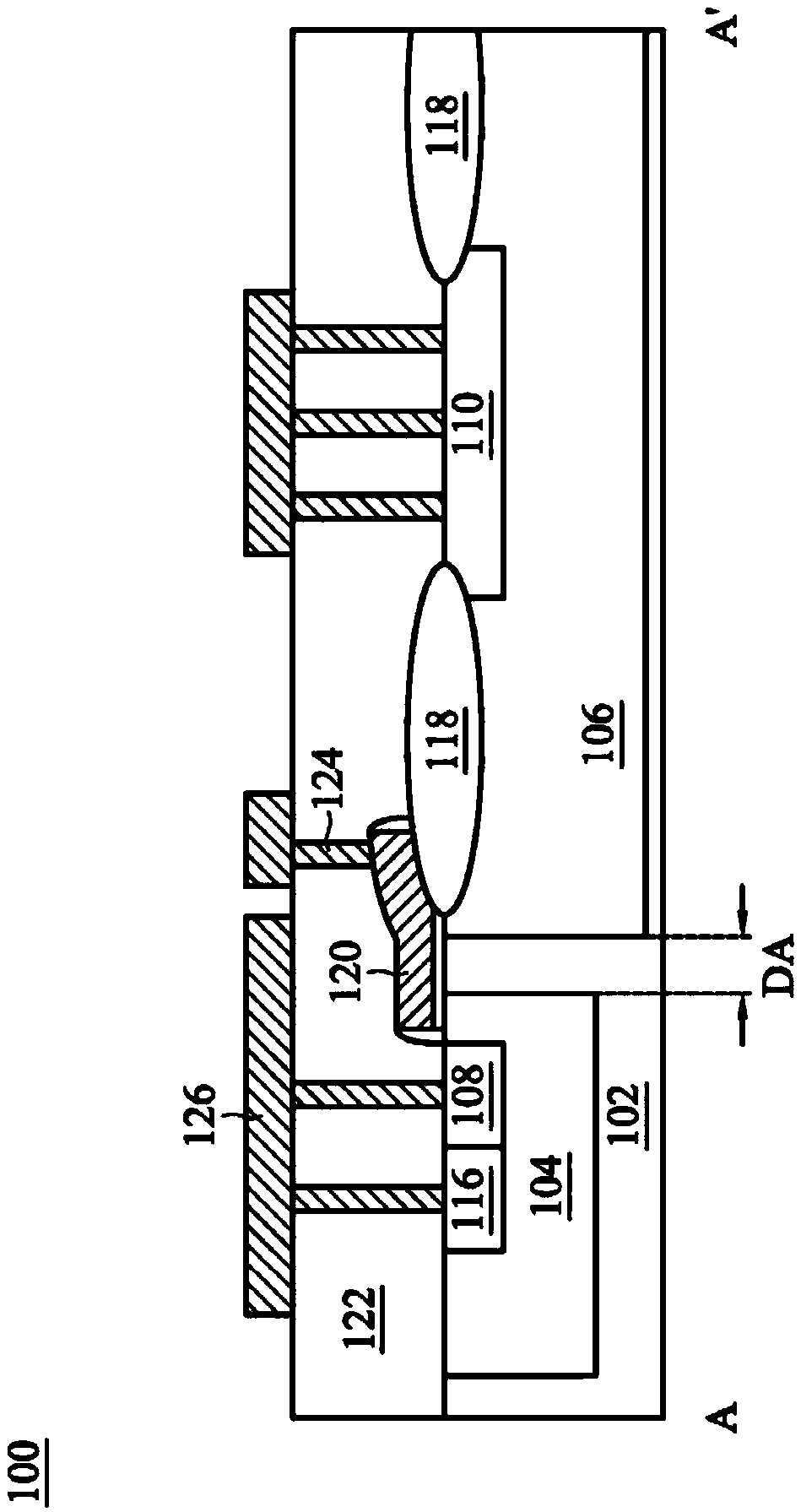
Figure 2 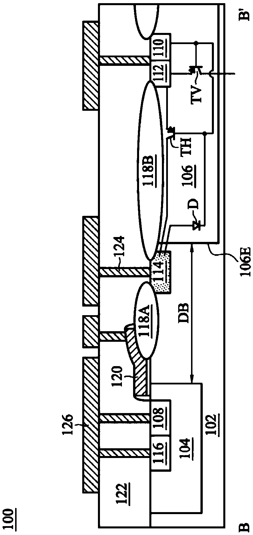
Figure 3
Abstract
Description
technical field
[0001] The embodiments of the present invention relate to a semiconductor technology, in particular to a laterally diffused metal oxide semiconductor field effect transistor. Background technique
[0002] High-voltage semiconductor components are suitable for high-voltage and high-power integrated circuits. Conventional high voltage semiconductor devices include lateral diffused metal oxide semiconductor field effect transistors (lateral diffused metal oxide semiconductor, LDMOS). The advantage of high-voltage semiconductor components is that they are easily compatible with other processes and are cost-effective, so they are widely used in power supplies, power management, display driver IC components, communications, automotive electronics, industrial control and other fields.
[0003] When the LDMOSFET is connected to an AC power source, a large amount of electrostatic charge may accumulate, and the electrostatic charge may flow at any two terminals to gen...
Examples
Embodiment Construction
[0046] Many different implementation methods or examples are disclosed below to implement different features of the embodiments of the present invention, and specific elements and embodiments of their arrangement are described below to illustrate the embodiments of the present invention. Of course, these embodiments are only for illustration, and should not limit the scope of the embodiments of the present invention. For example, it is mentioned in the description that the first feature is formed on the second feature, which includes the embodiment that the first feature is in direct contact with the second feature, and also includes other features between the first feature and the second feature. Embodiments of the features, that is, the first feature is not in direct contact with the second feature. In addition, repeated symbols or signs may be used in different embodiments, and these repetitions are only for the purpose of simply and clearly describing the embodiments of th...