
OLED circuit compensation method
A compensation method and circuit technology, applied in instruments, static indicators, etc., can solve problems such as poor pixel luminous effect, and achieve the effects of solving poor display effect, increasing yield, and reducing deterioration.
Patent Information
- Authority / Receiving Office
- CN · China
- Patent Type
- Applications(China)
- Current Assignee / Owner
- Publication Date
- 2020-02-21
- Estimated Expiration
- Not applicable · inactive patent
Smart Images
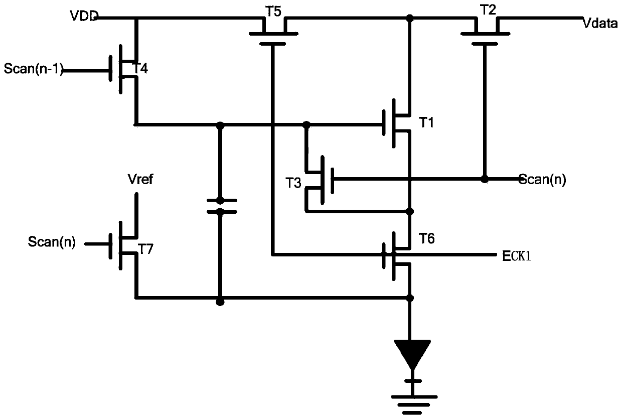
Figure 1 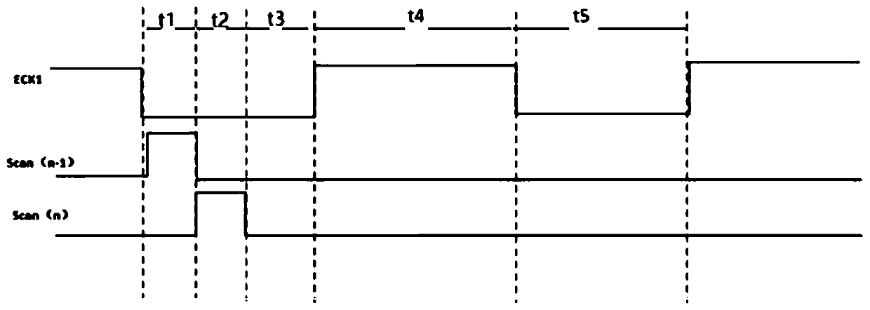
Figure 2 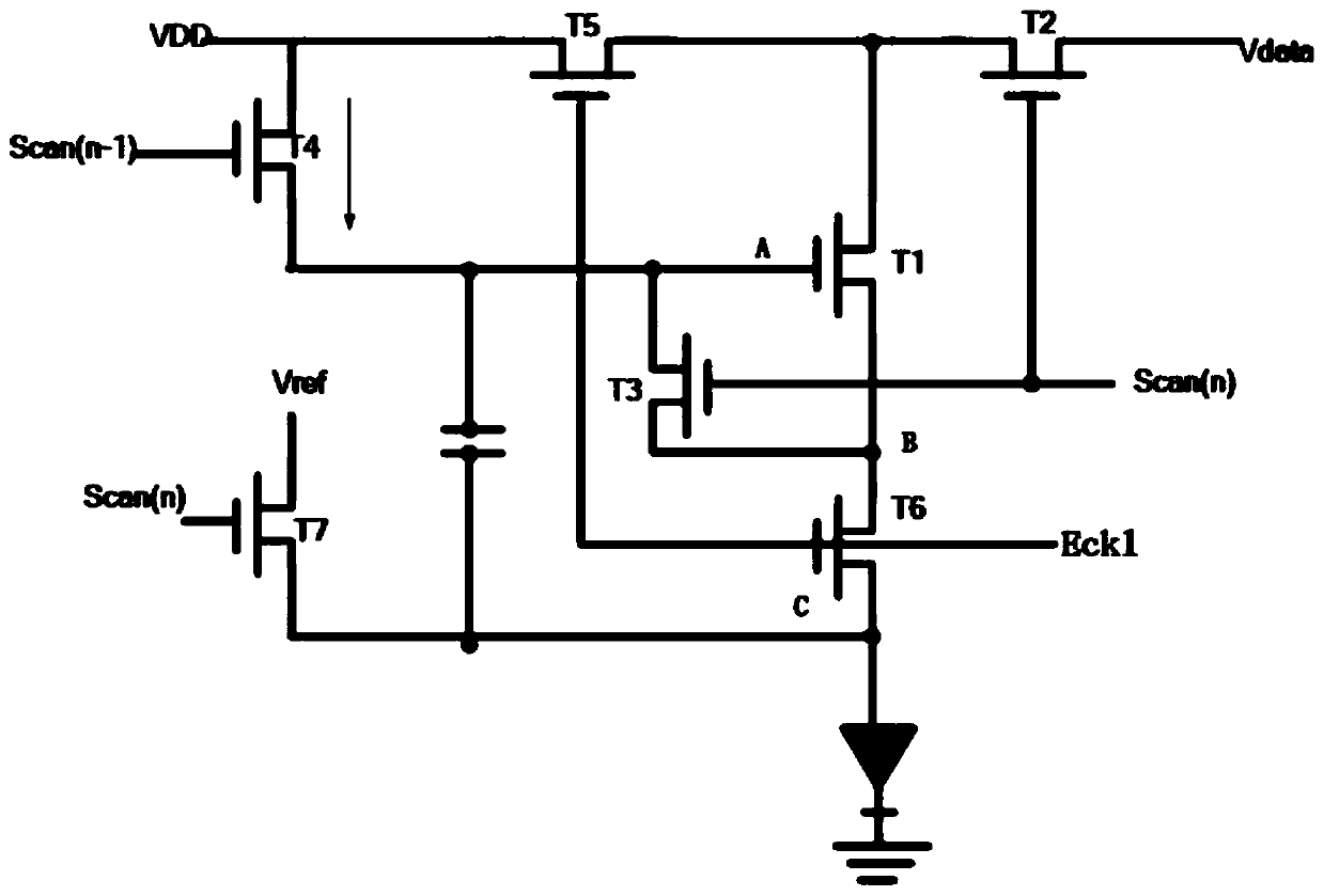
Figure 3
Abstract
Description
technical field
[0001] The invention relates to a pixel circuit display optimization technology, in particular to a novel OLED pixel driving compensation method. Background technique
[0002] Organic light emitting diodes (Organic Light Emitting Diode, OLED) can be divided into passive matrix driving (Passive Matrix OLED, PMOLED) and active matrix driving (Active Matrix OLED, AMOLED) according to the driving method. Among them, the PMOLED does not emit light when data is not written, but only emits light during data writing. This driving method is simple in structure, low in cost, and easy to design, and is mainly suitable for small and medium-sized displays.
[0003] Finally, AM stands for Active Matrix, which is relative to Passive Matrix and refers to the driving method of each OLED pixel. In Passive Matrix, the control of each pixel is realized through a complex electrode network, so as to realize the charge and discharge of a certain pixel. Generally speaking, the con...
Examples
Embodiment Construction
[0021] In order to explain in detail the technical content, structural features, achieved goals and effects of the technical solution, the following will be described in detail in conjunction with specific embodiments and accompanying drawings.
[0022] see figure 1 , a total of seven TFT transistors and a capacitor, that is, 7T1C design, the transistor is an N-type structure. We can see from the figure that an OLED circuit compensation method is characterized in that it is suitable for OLED circuits, and the OLED circuit includes thin film transistors T1, T2, T3, T4, T5, T6, T7, capacitor C1, power supply voltage VDD is connected to the source of T5 and the source of T4, the gate of T5 is connected to the gate of T6 and connected to the clock signal line, the drain of T5 is connected to the sources of T1 and T2; the T4 The gate of T3 is connected with the scan signal of the previous stage, and the drain is connected with the source of T3 and the gate of T1; the gate of T3 is...