
Flat coupling ridge waveguide semiconductor laser
A ridge waveguide and semiconductor technology, applied in the field of semiconductor laser devices, can solve the problems of high cavity surface power density, optical cavity surface catastrophe, narrow mode field area, etc., and achieve the goal of improving laser output power, good beam quality, and reducing power density Effect
Patent Information
- Authority / Receiving Office
- CN · China
- Current Assignee / Owner
- Publication Date
- 2021-11-26
Smart Images
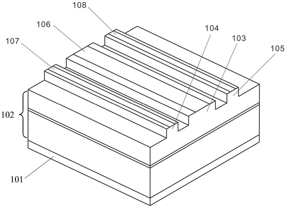
Figure 1
Abstract
Description
technical field
[0001] The invention belongs to the technical field of semiconductor laser devices, and in particular relates to a flat plate coupled ridge waveguide semiconductor laser. Background technique
[0002] Slab waveguide semiconductor lasers have the advantages of simple structure, high power, and low cost, and are widely used in laser medical treatment, free space optical communication, pump source, phased array radar, and advanced material processing. Among them, the slab waveguide semiconductor laser near the wavelength of 976nm is mainly used for the pumping of the ytterbium-doped fiber laser, which can obtain higher light-to-light conversion efficiency.
[0003] Although the current slab waveguide semiconductor lasers have high output power, they have multi-mode lasing, and the beam quality of the output laser is poor, which limits the application of slab waveguide semiconductor lasers. The main method to improve the beam quality is in slab waveguide semicond...
Examples
Embodiment 1
[0029] like figure 1 As shown, in this embodiment, a slab-coupled ridge waveguide semiconductor laser is specifically provided, aiming to further increase the total laser output power under the premise of maintaining better beam quality through optimization and improvement of the semiconductor laser. In this embodiment, a 976nm semiconductor laser is used, and the 976nm semiconductor laser mainly includes: a common electrode 101 and an epitaxial layer 102 that are stacked and arranged in sequence.
[0030] Three ridge waveguides are provided on the top of the epitaxial layer 102, respectively the first ridge waveguide 103, the second ridge waveguide 104 and the third ridge waveguide 105, wherein the first ridge waveguide 103 is a wide ridge waveguide and the second ridge waveguide 104 and The third ridge waveguide 105 is a narrow ridge waveguide, and the width of the narrow ridge waveguide is smaller than the width of the wide ridge waveguide. In this embodiment, the second r...
Embodiment 2
[0036]In this embodiment, a slab-coupled ridge waveguide semiconductor laser is specifically provided, aiming to further increase the total output power of the laser on the premise of maintaining better beam quality through optimization and improvement of the semiconductor laser. In Embodiment 1 On the basis, the design of the semiconductor laser is as follows:
[0037] Three ridge waveguides are provided on the top of the epitaxial layer 102, respectively the first ridge waveguide 103, the second ridge waveguide 104 and the third ridge waveguide 105, wherein the first ridge waveguide 103 is a wide ridge waveguide and the second ridge waveguide 104 And the third ridge waveguide 105 is a narrow ridge waveguide, the width of the narrow ridge waveguide is smaller than the width of the wide ridge waveguide. In this embodiment, the second ridge waveguide 104 and the third ridge waveguide 105 are located on both sides of the first ridge waveguide 103 and distributed asymmetrically. ...