
Discharge electrode, a discharge lamp and a method for manufacturing the discharge electrode
Patent Information
- Authority / Receiving Office
- US · United States
- Current Assignee / Owner
- Publication Date
- 2005-03-24
- Estimated Expiration
- Not applicable · inactive patent
Smart Images
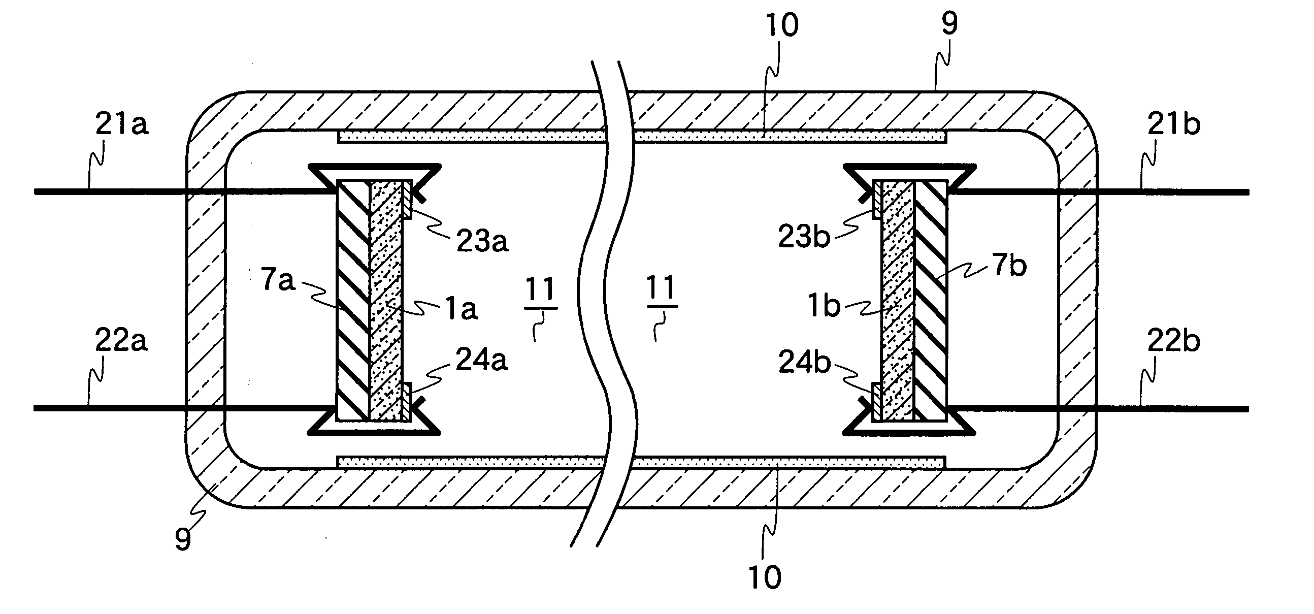
Figure 1 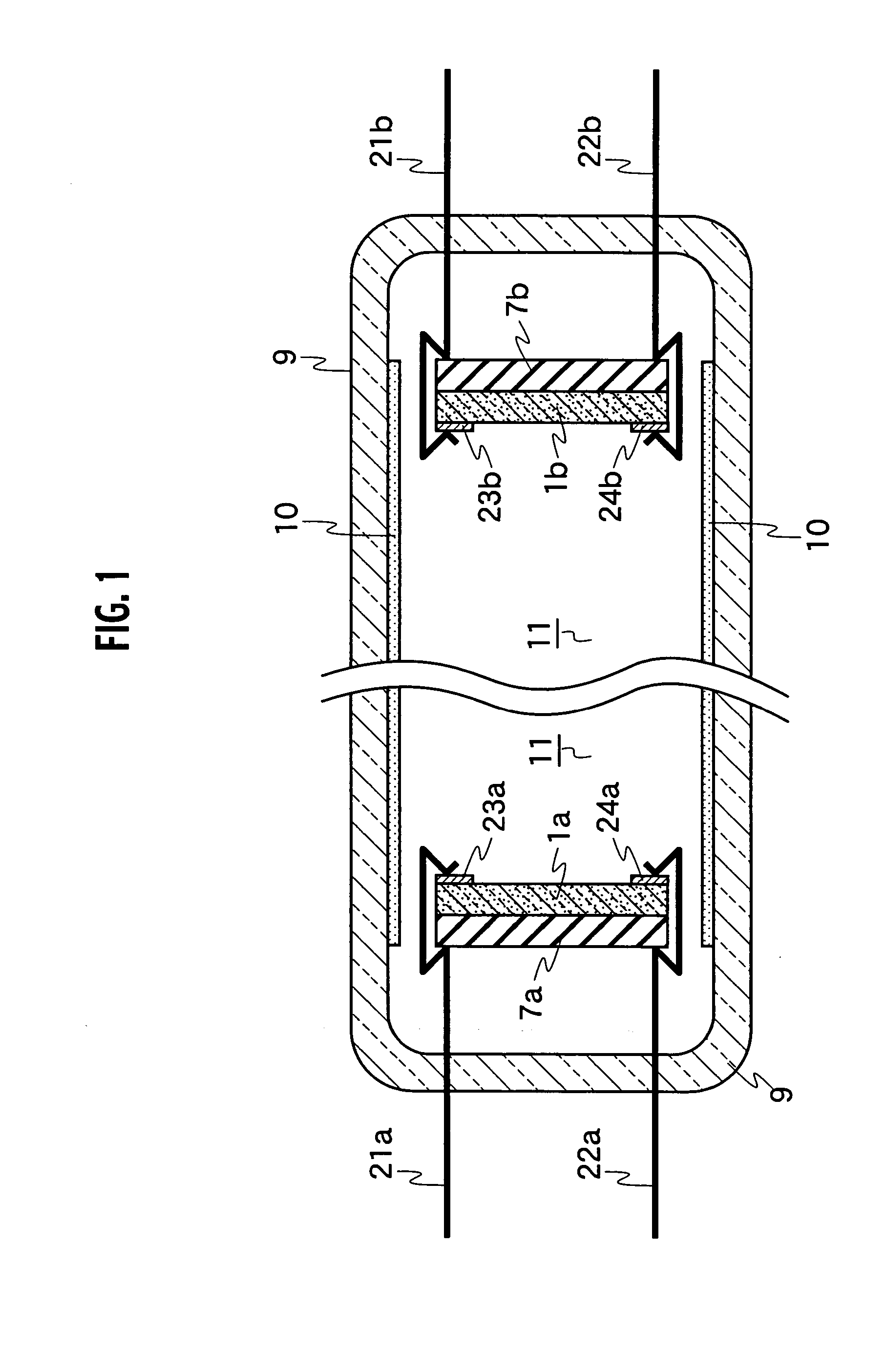
Figure 2 
Figure 3
Abstract
Description
CROSS REFERENCE TO RELATED APPLICATIONS
[0001] This application claims benefit of priority under 35 USC 119 based on Japanese Patent Application No. P2003-202518 filed Jul. 28, 2003, the entire contents of which are incorporated by reference herein. BACKGROUND OF THE INVENTION
[0002] 1. Field of the Invention
[0003] The present invention relates to a discharge electrode, a discharge lamp using the discharge electrode and a method for manufacturing the discharge electrode, and more particularly to a discharge electrode serving as a hot cathode, a discharge lamp using the discharge electrode and a method for manufacturing the discharge electrode.
[0004] 2. Description of the Related Art
[0005] A hot cathode (discharge electrode), used for discharge lamps such as fluorescent lamps, emit electrons from its surface in an atmosphere of a discharge gas by being thermally heated under application of negative potential to its surface. The hot cathode widely utilizes a filament implemented by...
Examples
first embodiment
[0032] (First Embodiment)
[0033] A discharge lamp pertaining to a first embodiment of the present invention, as indicated in FIG. 1, encompasses a discharge envelope 9 in which a discharge gas 11 is sealed, a fluorescent layer 10 with a thickness of 50 μm to 300 μm formed on a portion of the inner wall of the discharge envelope 9, and a pair of discharge electrodes placed at both the ends of the discharge envelope 9 therein The discharge envelope 9 can utilize, for example, a glass tube composed of soda lime glass and borosilicate glass and the like.
[0034] Of the pair of discharge electrodes, the discharge electrode of the left side in FIG. 1 encompasses an insulating substrate 7a serving as a supporting member, and a wide bandgap semiconductor layer 1a, which serves as an emitter formed on the insulating substrate 7a. On the top surface of the wide bandgap semiconductor layer (emitter) 1a conductive films (contact films) 23a, 24a that implement a low-contact-resistance ohmic contac...
second embodiment
[0059] (Second Embodiment)
[0060] As shown in FIG. 11, a discharge electrode of a discharge lamp relating to a second embodiment of the present invention encompasses a wide bandgap semiconductor rod 12 serving as an emitter, conductive films (contact films) 31a, 31b selectively formed at outer peripheries of vicinities of both the ends of the wide bandgap semiconductor rod 12, a lead wire 13a wound around the left side end of the wide bandgap semiconductor rod 12 through the conductive film (contact film) 31a, and a lead wire 13b wound around the right-hand side end of the wide bandgap semiconductor rod 12 through the conductive film (contact film) 31b.
[0061] The wide bandgap semiconductor rod 12 is a pillar-shaped rod, which can establish a prism shape having an edge of 50 μm to 300 μm, or a cylindrical shape having a diameter of 50 μm to 300 μm. The prism shape does not necessarily have a square in cross section; the cross-sectional shape may be a rectangle, or a pentagon or a pol...
third embodiment
[0067] (Third Embodiment)
[0068] As indicated in FIG. 13, a discharge electrode of a discharge lamp relating to a third embodiment of the present invention encompasses a cylindrical insulating core member 18 serving as a supporting member and a wide bandgap semiconductor layer 17 coating on the entire outer surface of the insulating core member 18, serving as an emitter, both implementing a cylindrical composite electrode-body (17, 18). Instead of the cylindrical insulating core member 18, a prism-shaped insulating core member 18 can be used as the supporting member, and in this case, a prism-shaped composite electrode-body (17, 18) will be established instead of the cylindrical composite electrode-body (17, 18).
[0069] The discharge electrode encompasses cap-shaped conductive films (electrode layers) 19a, 19b selectively formed at the outer peripheries of both edges of the wide bandgap semiconductor layer (emitter) 17, an electrode pin 20a welded at the conductive film (electrode la...