
Voltage controlled clock synthesizer
Patent Information
- Authority / Receiving Office
- US · United States
- Current Assignee / Owner
- Publication Date
- 2006-06-08
Smart Images
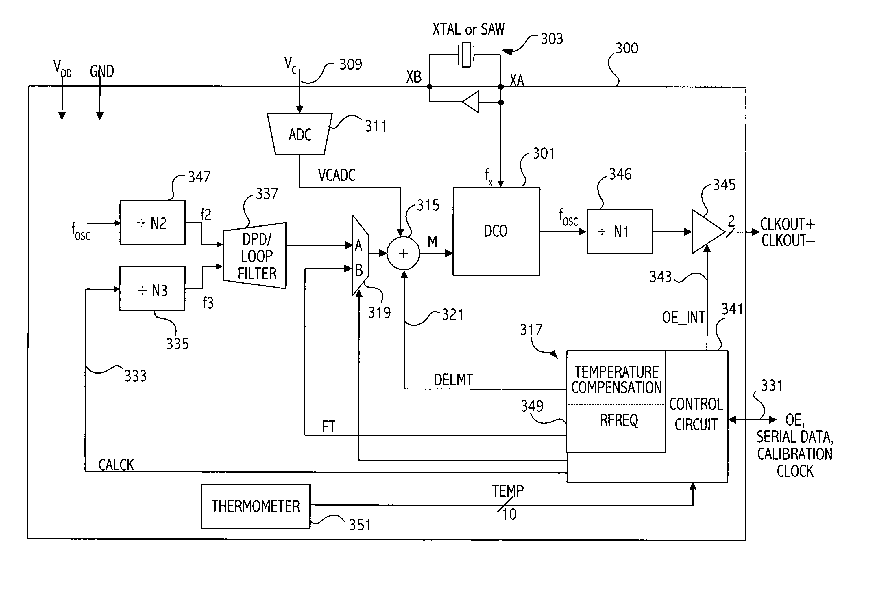
Figure 1 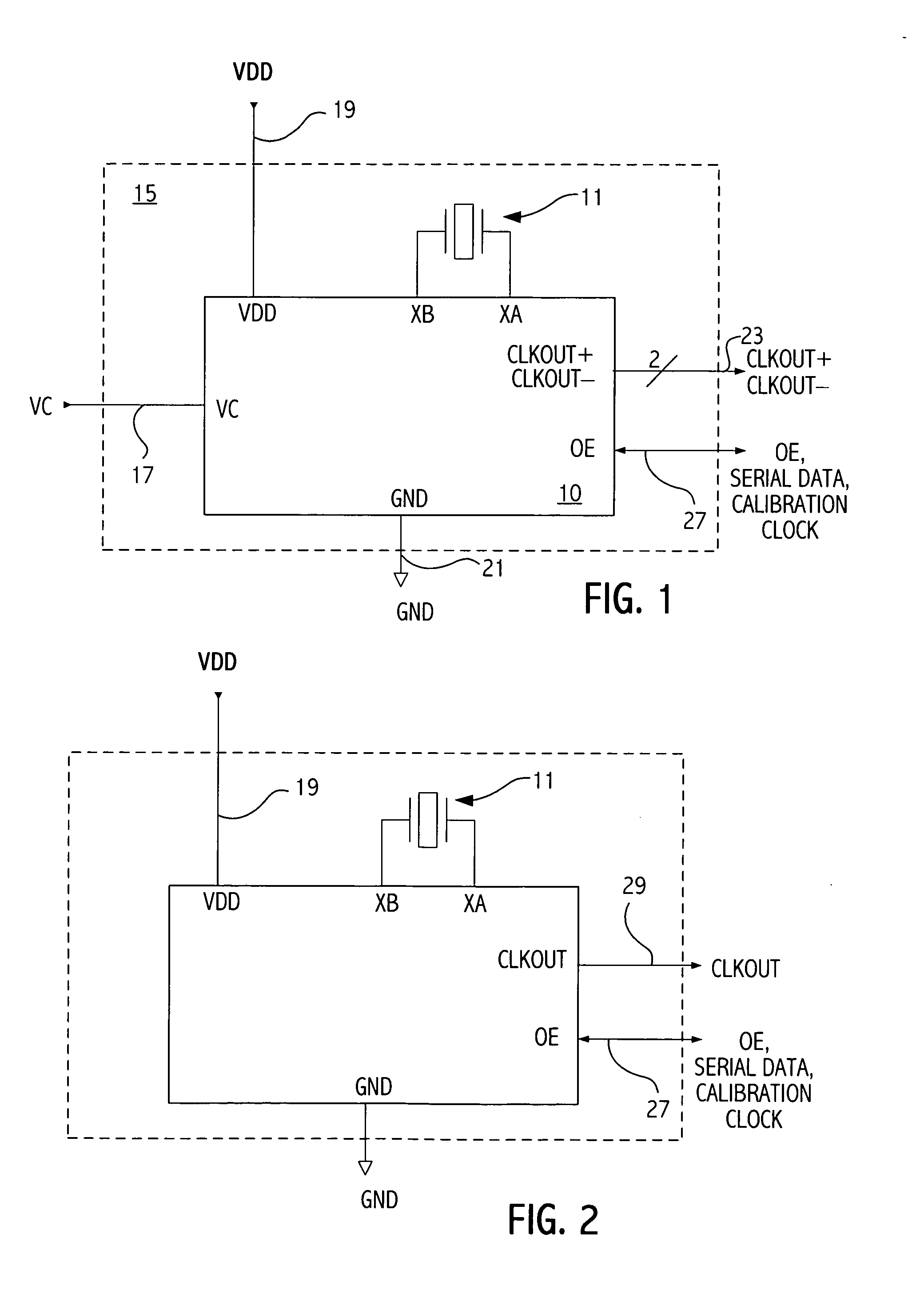
Figure 2 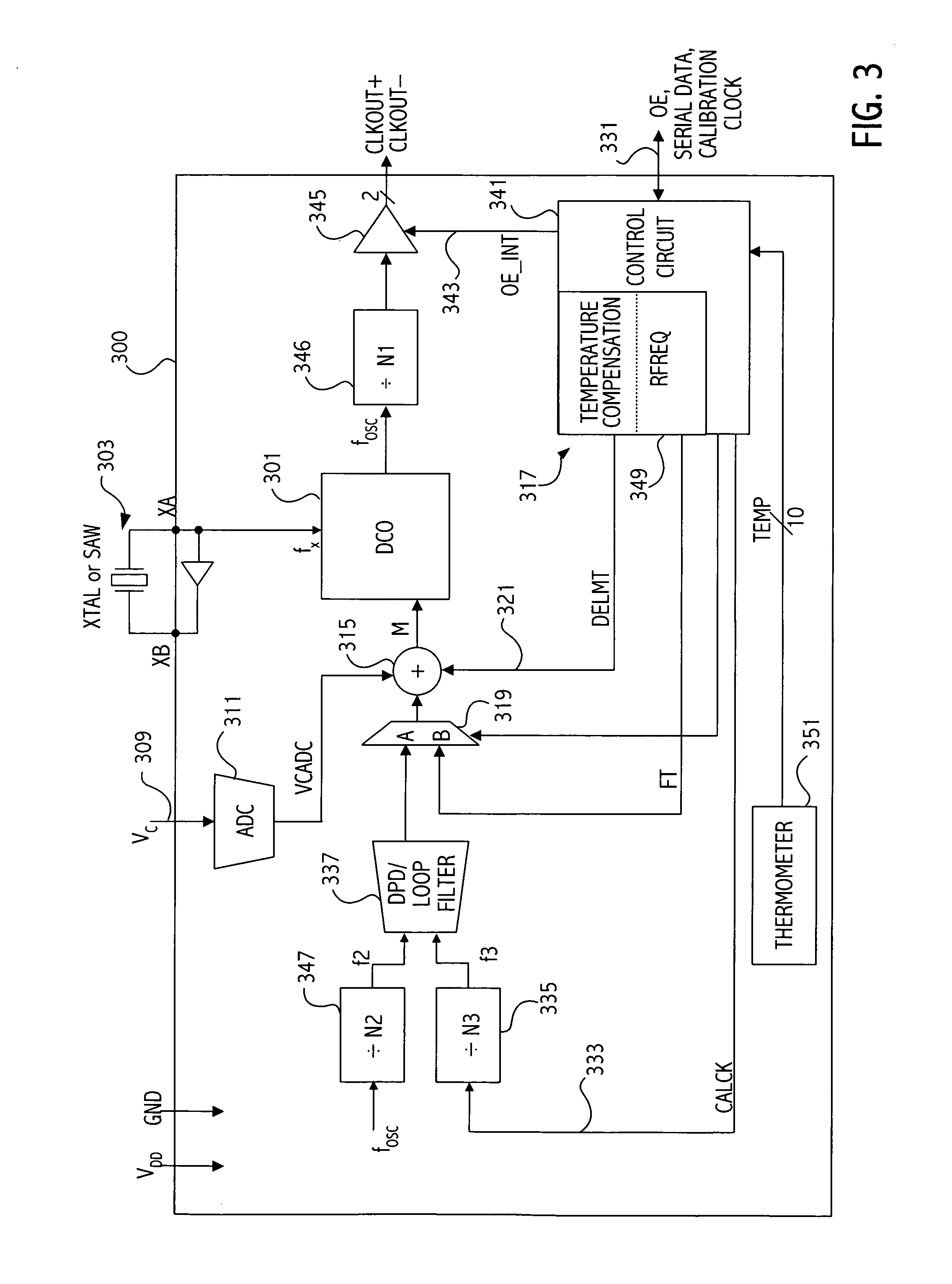
Figure 3
Abstract
Description
[0001] This application is a continuation in part of application Ser. No. 10 / 878,218, filed Jun. 28, 2004, which application claims benefit under 35 U.S.C. 119(e) of application 60 / 567,479, entitled “METHOD AND APPARATUS FOR A PROGRAMMABLE CLOCK SOURCE GENERATING A WIDE RANGE OF OUTPUT FREQUENCIES”, filed May 3, 2004, naming Axel Thomsen, Yunteng Huang, Jerrell P. Hein as inventors, and which application is a continuation-in-part of application Ser. No. 10 / 675,543, entitled “CALIBRATION OF OSCILLATOR DEVICES”, filed Sep. 30, 2003, naming Jerrell Hein and Axel Thomsen as inventors, which claimed benefit under 35 U.S.C. §119(e) of application 60 / 467,813, filed May 2, 2003; which applications are incorporated herein by reference.BACKGROUND
[0002] 1. Field of the Invention
[0003] This application relates to integrated circuit devices more particularly to integrated circuits utilized in generating clock signals and systems incorporating such circuits.
[0004] 2. Description of the Related...
Examples
Embodiment Construction
)
[0037] Referring to FIG. 1, a high level diagram shows a clock source device that includes an integrated circuit 10 coupled to a crystal 11. In one embodiment both the integrated circuit 10 and the crystal 11 are packaged in a standard ceramic package 15 that is typically utilized for packaging a voltage controlled crystal oscillator (VCXO). Note that another resonating device such as a surface acoustic wave (SAW) resonator may be utilized in place of crystal 11. In the illustrated embodiment, the package 15 includes standard input / output signals including a voltage control input 17, a power and ground input, 19 and 21 respectively, differential clock outputs and an output enable (OE) pin 27. FIG. 2 illustrates a four pin XO package implementation in which the control voltage input 17 is not utilized and the output clock 29 is single ended. A six pin XO package configuration may also be utilized in which the control voltage input on the package is not connected when the package 15 ...