
Architecture and method for providing integrated circuits
Patent Information
- Authority / Receiving Office
- US · United States
- Current Assignee / Owner
- Publication Date
- 2007-10-11
- Estimated Expiration
- Not applicable · inactive patent
Smart Images
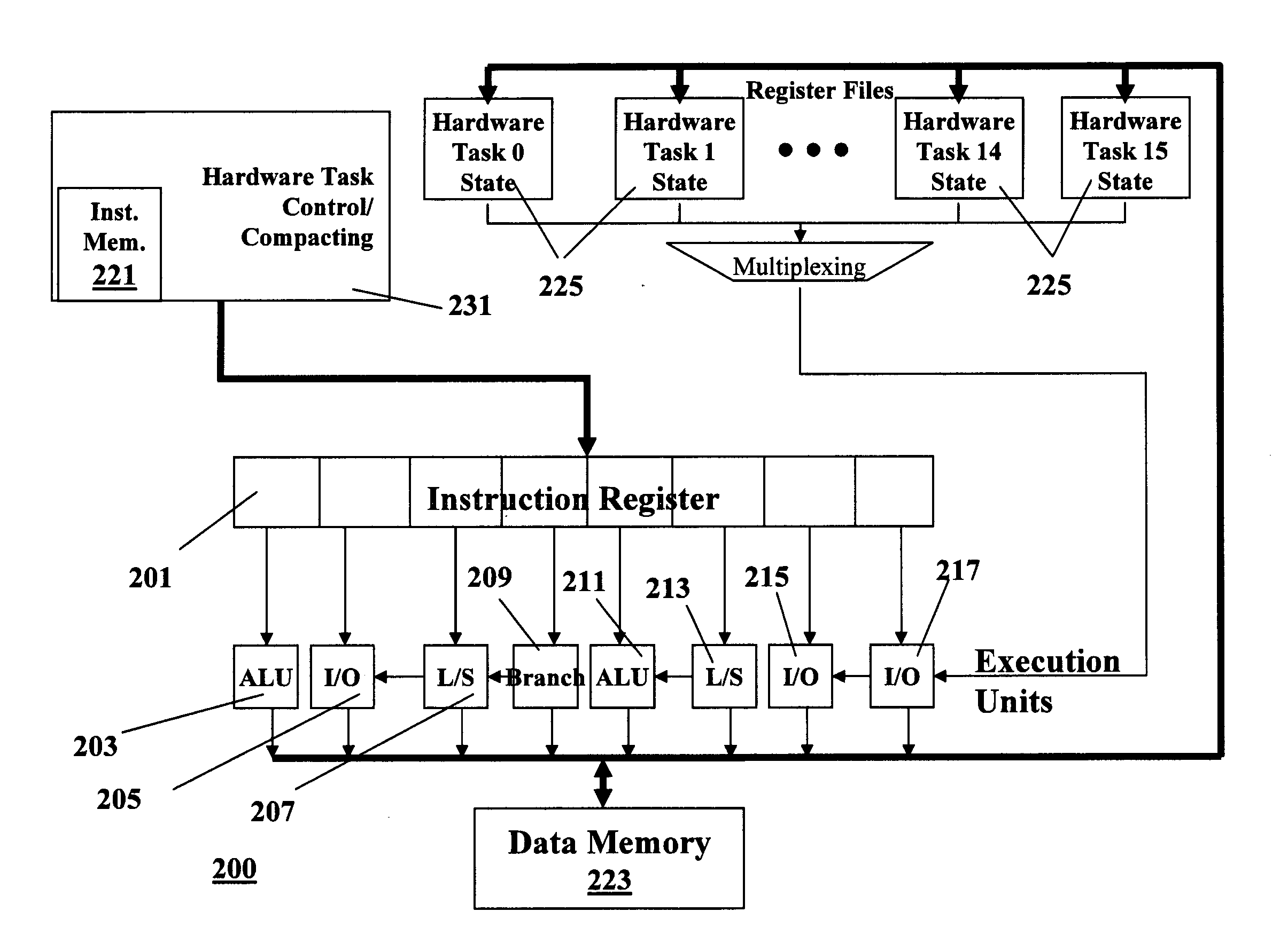
Figure 1 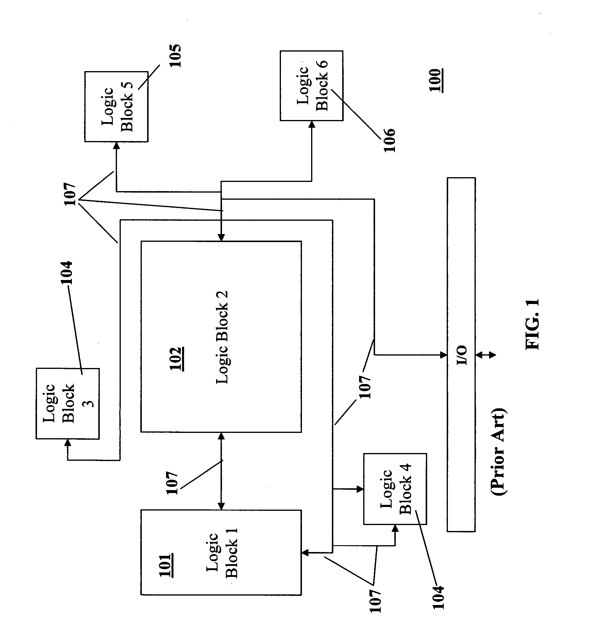
Figure 2 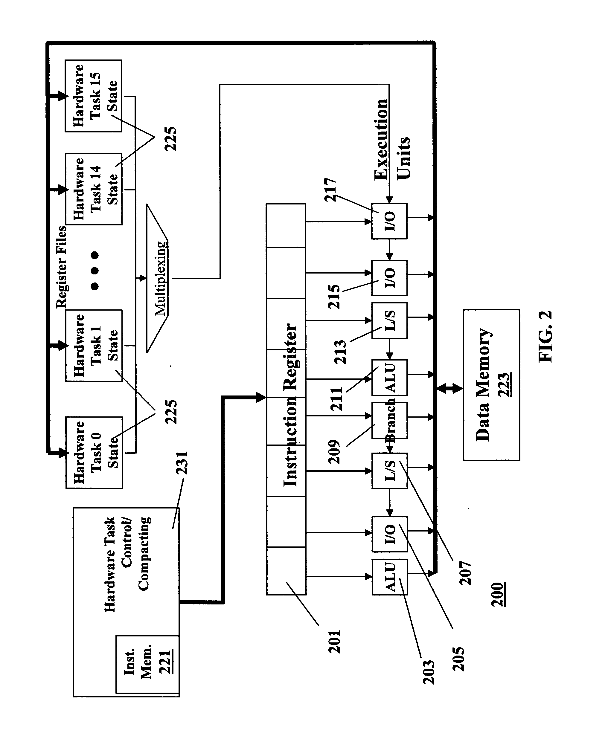
Figure 3
Abstract
Description
RELATED APPLICATIONS
[0001] This application claims the benefit of and priority based upon U.S. provisional application for patent 60 / 790,637 filed on Apr. 10, 2006.FIELD OF THE INVENTION
[0002] The invention pertains to integrated circuit design, in general, and to a system and method of providing customized integrated circuits, in particular. BACKGROUND OF THE INVENTION
[0003] There is a demand for customized Integrated Circuits (“ICs”). Customization allows companies to differentiate themselves from the competition by placing specialized, user-specific functions on the IC. Though custom lCs have existed since the dawn of the semiconductor industry, the effects of Moore's law have increased the complexity of ICs to such an extent that the nature of the design has changed. Those changes will continue in the future, creating a need to improve design productivity dramatically.
[0004] Designing a custom chip is an exercise in defining two items: (a) logic, which takes input signals, p...
Examples
first embodiment
[0034] A first embodiment architecture in accordance with the principles of the invention is shown in FIG. 2. The architecture of FIG. 2 is a meta-processor 200 that allows concurrent execution of many tasks. It is based on a Very Long Instruction Word (VLIW) architecture, which has natural concurrency as part of the architecture. Users of the present invention design the hardware functions with software tools, dramatically reducing development costs.
[0035] The architecture of the present invention is a VLIW meta-processor that is a super ‘bit-bang’ machine, i.e., a processor that toggles the I / O of a chip using software, rather than hardware. Logic is implemented in software, running the algorithms that today's ASICs and FPGAs perform in hardware. Interconnect is implemented through memory mailboxes between programs. Both are described in more detail below.
[0036] VLIW processors differ from typical processors, e.g. the x86 series, in the length of the instruction word. Typical pro...
second embodiment
[0079]FIG. 14 shows a second embodiment architecture in accordance with the principles of the invention, meant to perform the functions in FIG. 13. A difference in architecture is the addition of instruction memory 221 on-chip, outside of the task control / compacting unit 231. This is because the hardware tasks will be much more complicated, especially when running processor code. Thus the code for each hardware task is located in the instruction memory 221 while the task control / compacting unit 231 contains cache instead of simple instruction memory.
[0080] The instruction length is 512 bits, made up of sixteen 32-bit instructions as shown in FIG. 15. It is substantially the same as the logic-only embodiment, with 32-bit-wide instruction words instead of 16.
[0081] Execution units 203, 1401, 205, 207, 209, 211, 213, 215, 217 are substantially identical to the logic-only version, except they are all 32-bit wide instead of 16 or 12.
[0082] The hardware task code is generated in an iden...