

Patterning process and method of manufacturing organic thin film transistor using the same
a technology patterning process, which is applied in the direction of basic electric elements, electrical apparatus, semiconductor devices, etc., can solve the problems of increasing the difficulty of high precision, reducing the performance of organic thin film transistor b>100/b>, and creating additional problems, etc., to achieve the effect of greater pattern precision
Patent Information
- Authority / Receiving Office
- US · United States
- Patent Type
- Applications(United States)
- Current Assignee / Owner
- Publication Date
- 2007-11-15
- Estimated Expiration
- Not applicable · inactive patent
Smart Images
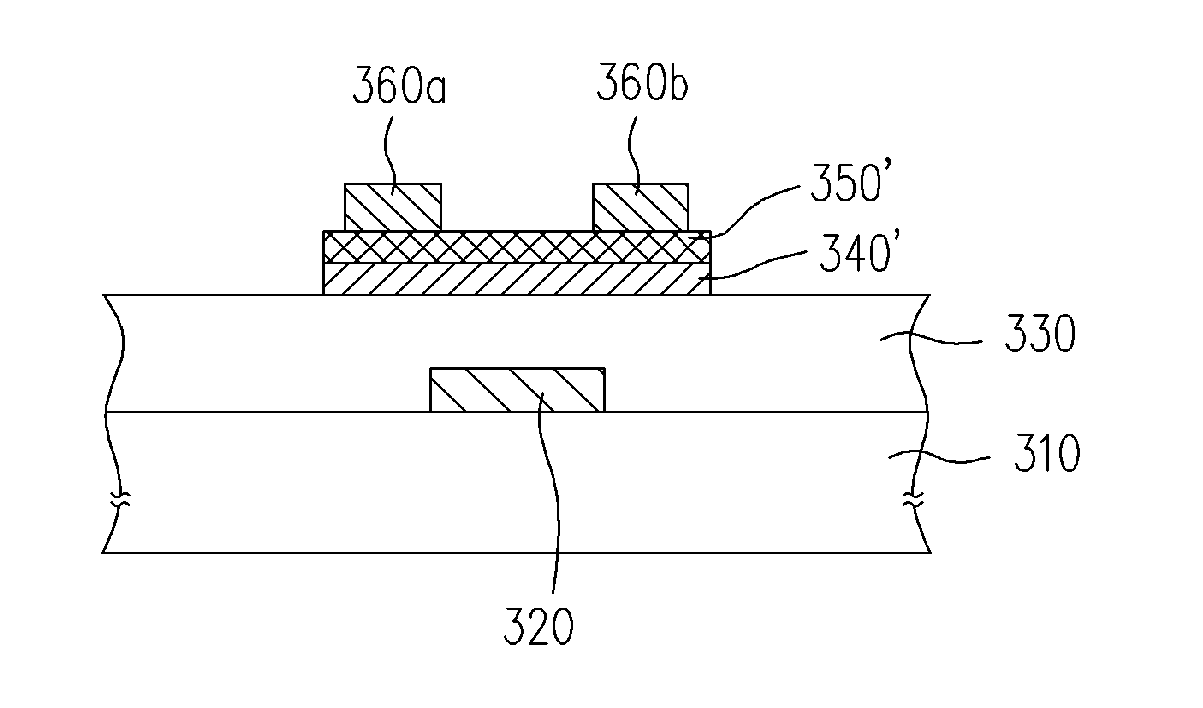
Figure 1 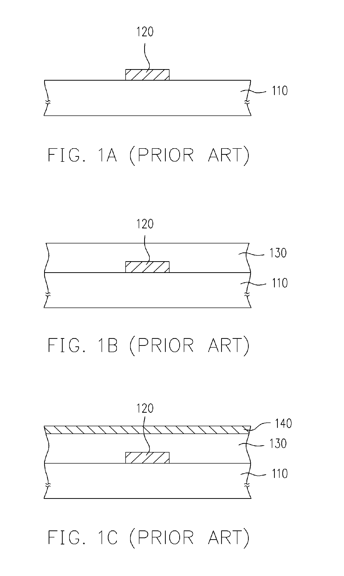
Figure 2 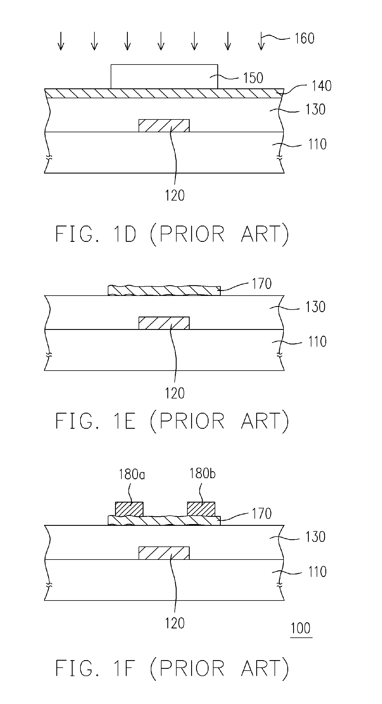
Figure 3
Abstract
Description
BACKGROUND OF THE INVENTION
[0001] 1. Field of the Invention
[0002] The present invention relates to a patterning process and a method of manufacturing an organic thin film transistor using the same. More particularly, the present invention relates to a patterning process using a self-assembled monolayer (SAM) and a method of manufacturing an organic thin film transistor (O-TFT) using the patterning process.
[0003] 2. Description of Related Art
[0004] Because organic semiconductor devices can be fabricated on a flexible plastics substrate or a thin metal substrate, it has the advantages of being light, cheap and flexible. Among the organic semiconductor devices, organic thin film transistor (O-TFT) has become one of the most important devices both in the academic circle and among industrial researchers in technically advanced countries.
[0005] FIGS. 1A through 1F are schematic cross-sectional views showing the steps of fabricating a conventional organic thin film transistor. First, a...
Examples
Embodiment Construction
[0039] Reference will now be made in detail to the present preferred embodiments of the invention, examples of which are illustrated in the accompanying drawings. Wherever possible, the same reference numbers are used in the drawings and the description to refer to the same or like parts.
[0040] The patterning process and the method of forming the organic thin film transistor in the present invention utilizes a self-assembled monolayer to define an organic material layer with a greater pattern precision. Furthermore, the interface characteristic of the organic material layer is also improved through the self-assembled monolayer. The following illustrations are just some of the preferred embodiments of the present invention and should not be used to limit the scope of the present invention.
[0041]FIGS. 2A through 2G are schematic cross-sectional views showing the steps in a patterning process according to one preferred embodiment of the present invention. First, as shown in FIG. 2A, ...