
Phase change random access memory and related methods of operation
a random access memory and phase change technology, applied in static storage, digital storage, instruments, etc., can solve the problems of not being able to simultaneously program the bits into corresponding memory cells, conventional pram devices are generally not equipped to provide currents of such high magnitudes, and achieve the effect of improving the efficiency and reliability of the devi
Patent Information
- Authority / Receiving Office
- US · United States
- Patent Type
- Applications(United States)
- Current Assignee / Owner
- Publication Date
- 2008-03-06
Smart Images
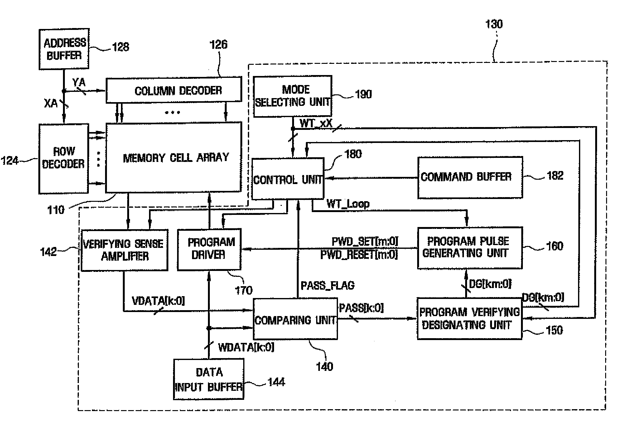
Figure 1 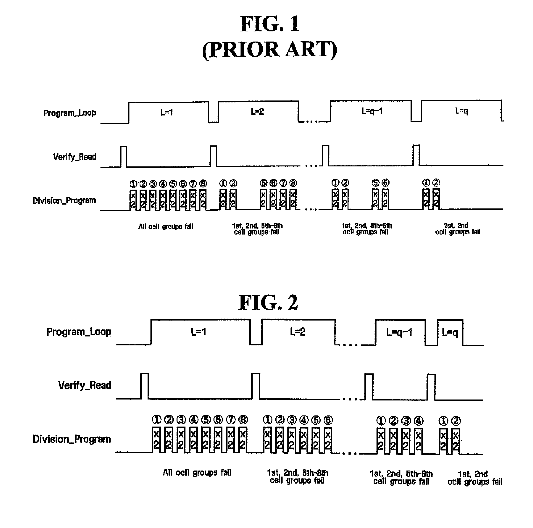
Figure 2 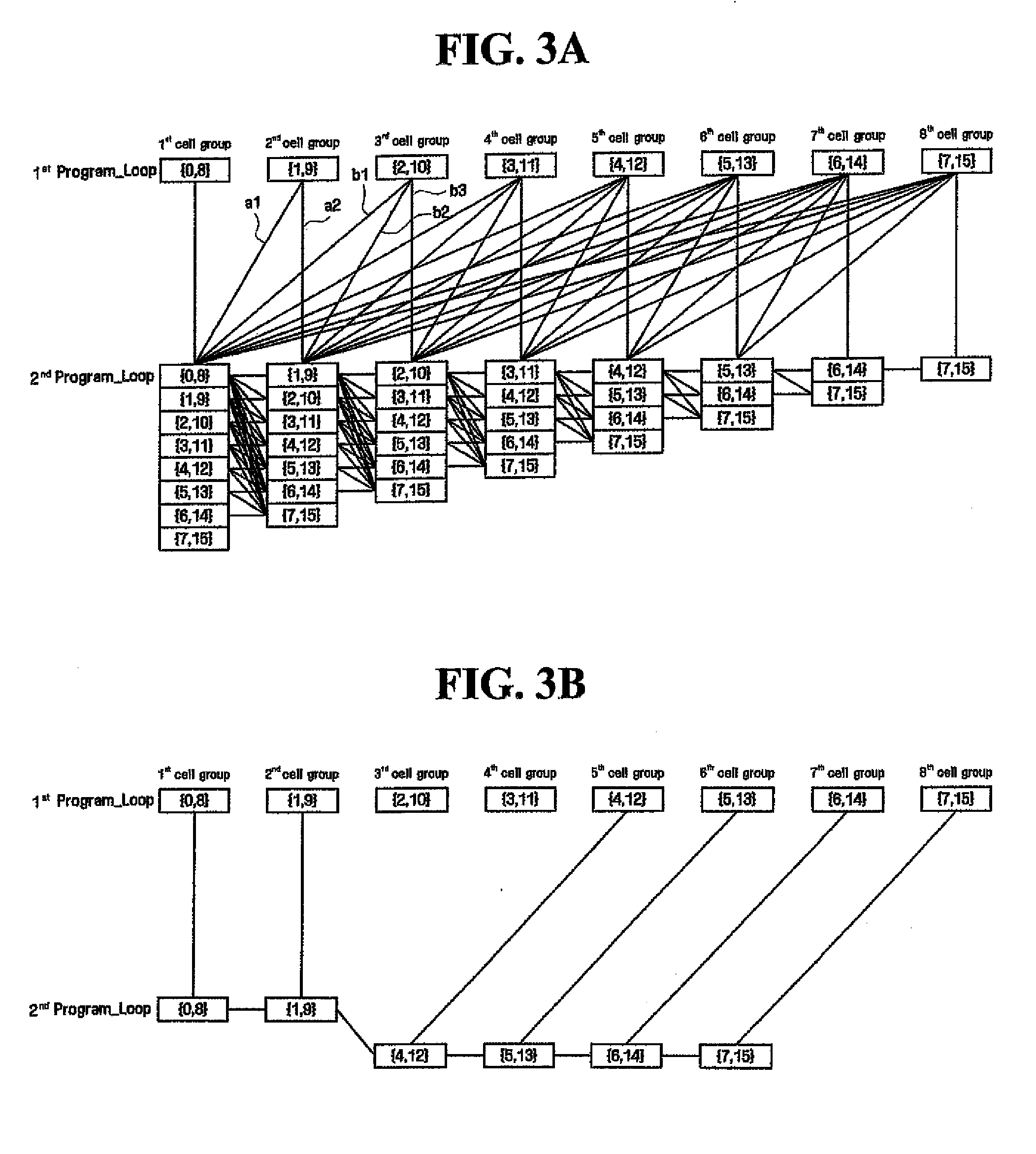
Figure 3
Abstract
Description
CROSS REFERENCE TO RELATED APPLICATIONS
[0001] This application claims the priority of Korean Patent Application No. 10-2006-0084863 filed on Sep. 4, 2006, the disclosure of which is hereby incorporated by reference in its entirety.BACKGROUND OF THE INVENTION
[0002] 1. Field of the Invention
[0003] Embodiments of the invention relate generally to phase change random access memory (PRAM) devices and related methods of operation. More particularly, embodiments of the invention relate to PRAM devices and related methods of performing program operations including divisional program operations and verify read operations.
[0004] 2. Description of Related Art
[0005] Phase change memory devices store data using phase change materials, such as chalcogenide, which are capable of stably transitioning between amorphous and crystalline phases. The amorphous and crystalline phases (or states) exhibit different resistance values used to distinguish different logic states of memory cells in the memory device...
Examples
Embodiment Construction
[0038]Exemplary embodiments of the invention are described below with reference to the corresponding drawings. These embodiments are presented as teaching examples. The actual scope of the invention is defined by the claims that follow.
[0039]FIG. 2 is a conceptual timing chart illustrating a method of performing a program operation in a PRAM device according to an embodiment of the invention.
[0040]Referring to FIG. 2, data is programmed to the PRAM device using a plurality of program loops. Before each program loop, a verify read operation is performed to determine whether selected memory cells have been successfully programmed. In this written description, data to be programmed in selected memory cells will be referred to as program data, and data read from the selected memory cells in a verify read operation will be referred to as verification data.
[0041]In each program loop, program data is programmed to selected cells using a plurality of divisional program operations correspond...