
Layout and schematic diagram consistency comparison method for multi-voltage chip design
A chip design, multi-voltage technology, applied in the direction of electrical digital data processing, calculation, special data processing applications, etc., can solve the problems that LVS cannot reflect the real situation, LVS cannot reflect the situation, and the efficiency of LVS is low, so as to save physical verification The effect of shortening time, shortening time, improving efficiency and reliability
Patent Information
- Authority / Receiving Office
- CN · China
- Current Assignee / Owner
- Publication Date
- 2012-07-18
Smart Images
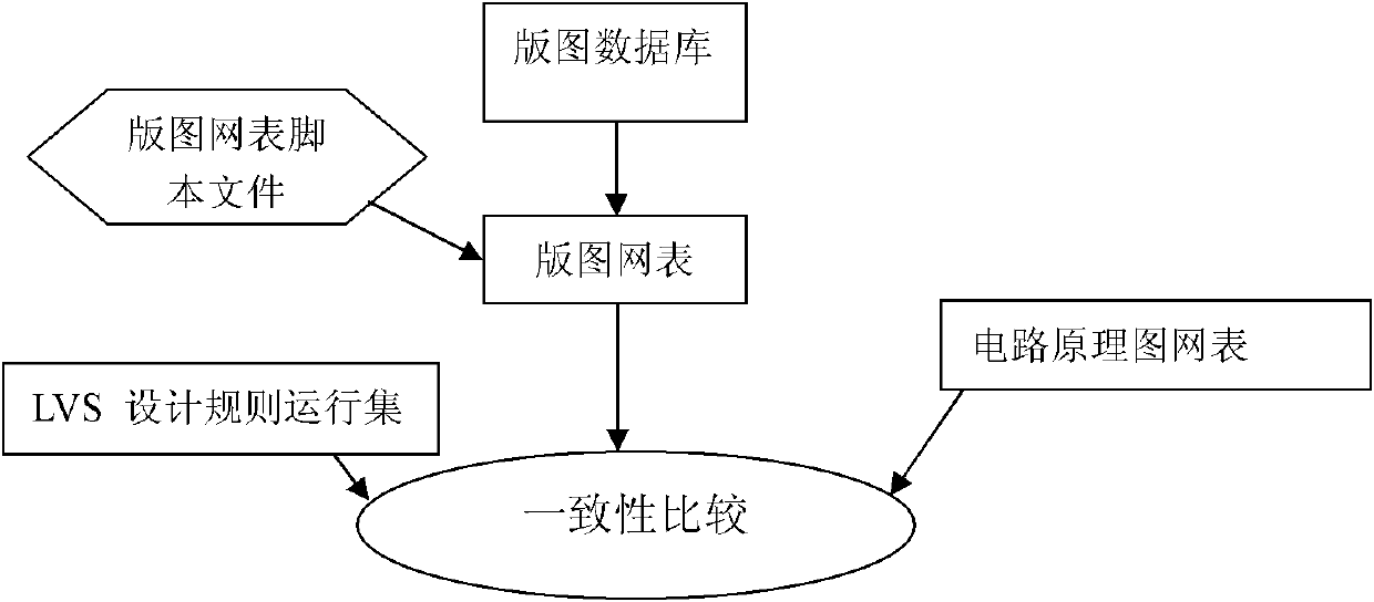
Figure 1 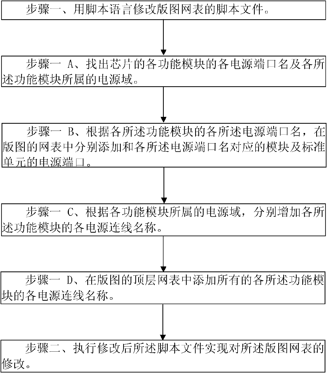
Figure 2 
Figure 3
Abstract
Description
technical field
[0001] The present invention relates to the field of semiconductor integrated circuit manufacturing, in particular to the layout and principle of a multi-voltage chip design Figure 1 consistency comparison method. Background technique
[0002] In the existing chip design, the layout and principle must be carried out after the chip layout design is completed. Figure 1 Consistency comparison (Layout versus Schematic, LVS) to ensure the consistency of layout and circuit schematic. Such as figure 1 As shown, it is the flow chart of the existing LVS, the steps of the existing LVS include the steps of extracting the layout netlist (Layout Netlist) from the layout database (Layout Database), and performing the comparison under the environment of the LVS design rule run set (Runset) A step of performing a consistency comparison (Compare) between the layout netlist and the schematic netlist (Schematic Netlist). The layout netlist can also be modified through a la...
Examples
Embodiment Construction
[0022] Such as figure 2 Shown is the flowchart of the method of the present invention, the layout and principle of the multi-voltage chip design of the embodiment of the present invention Figure 1 The consistency comparison method includes the following steps:
[0023] Step 1: Use PERL language to modify the script file MPower.pl of the layout netlist. The following steps are included when modifying the MPOwer.pl:
[0024] Step 1A. Find out the name of each power port of each functional module of the chip and the power domain to which each power port belongs. Each of the functional modules includes two types of power normally-on modules and power-off modules.
[0025] Step 1B. According to the names of the power ports of the functional modules, add the modules corresponding to the names of the power ports and the power ports of the standard cells in the layout netlist.
[0026] Step 1C. According to the power domain to which each functional module belongs, add the name of...