
Computing device and method of checking wiring diagrams of PCB
a computing device and wiring diagram technology, applied in computing, error detection/correction, instruments, etc., can solve the problems of inefficiency, cost, complicated,
Patent Information
- Authority / Receiving Office
- US · United States
- Current Assignee / Owner
- Publication Date
- 2014-06-19
- Estimated Expiration
- Not applicable · inactive patent
Smart Images
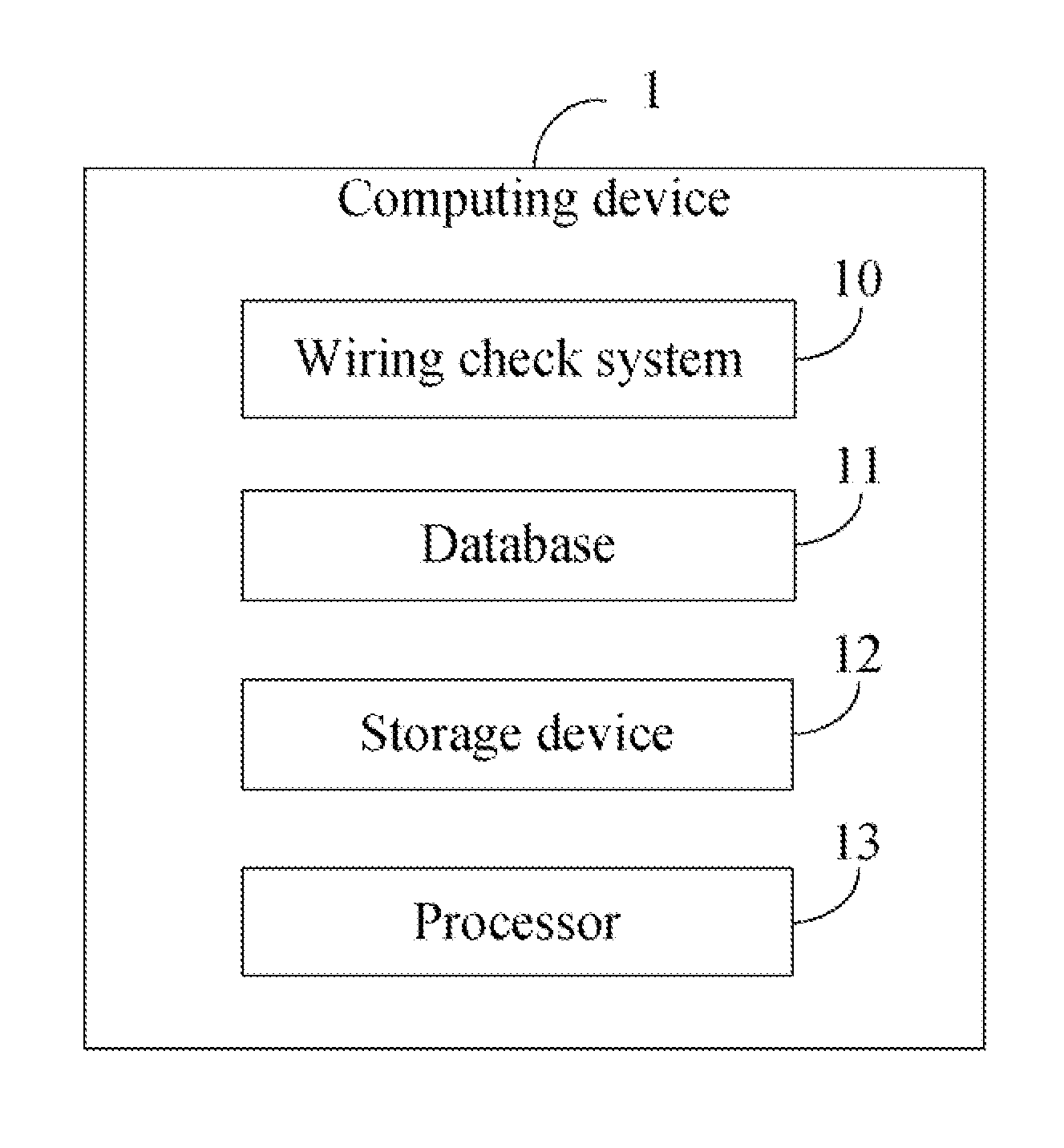
Figure 1 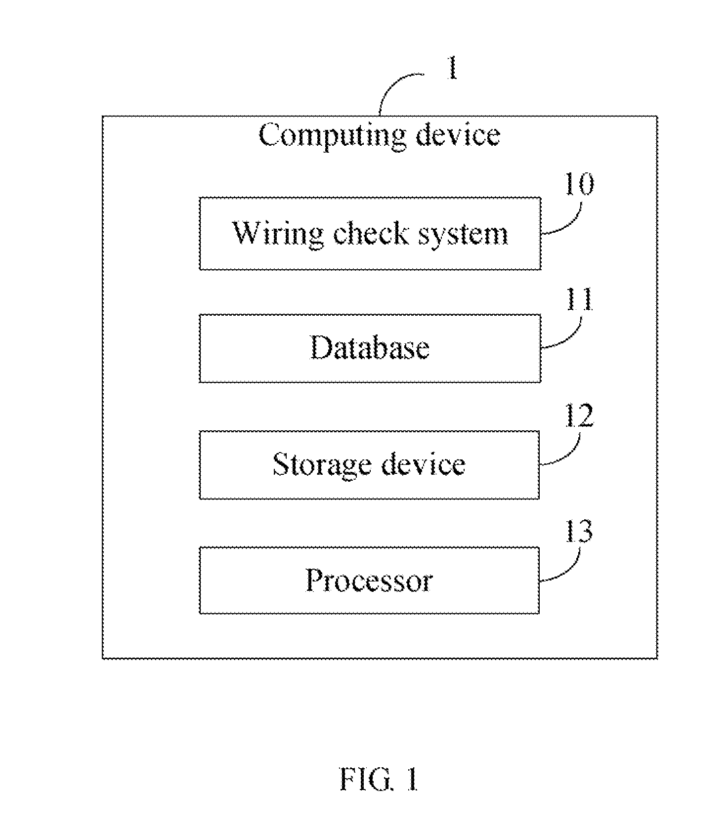
Figure 2 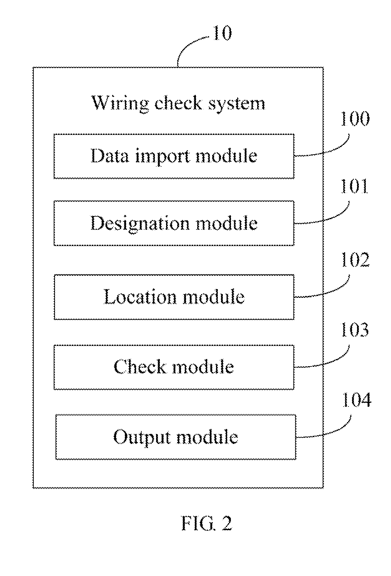
Figure 3
Abstract
Description
BACKGROUND
[0001] 1. Technical Field
[0002] Embodiments of the present disclosure relate to wiring design, and more particularly to a computing device and a method of checking wiring diagrams of a printed circuit board (PCB) design.
[0003] 2. Description of Related Art
[0004] Electronic devices, such as mobile phones and computers, may include one or more printed circuit boards (PCBs). The PCB mechanically supports and electrically connects electronic components, such as resistors, capacitors, using signal lines. In order to assure the stability and reliability of a PCB, it is necessary to perform a series of checks of the wiring of the PCB. In traditional check methods, the check may be performed manually, which may be complicated, inefficient, and costly. Therefore, a more efficient system and method for checking wiring of a PCB layout file is desired.BRIEF DESCRIPTION OF THE DRAWINGS
[0005] FIG. 1 is a block diagram of one embodiment of a computing device including a wiring check system.[0...
Examples
Embodiment Construction
[0008]In general, the word “module,” as used hereinafter, refers to logic embodied in hardware or firmware, or to a collection of software instructions, written in a programming language, such as, for example, Java, C, or Assembly. One or more software instructions in the modules may be embedded in firmware. It will be appreciated that modules may comprised connected logic units, such as gates and flip-flops, and may comprise programmable units, such as programmable gate arrays or processors. The modules described herein may be implemented as either software and / or hardware modules and may be stored in any type of computer-readable medium or other computer storage device.
[0009]FIG. 1 is a block diagram of one embodiment of a computing device 1 including a wiring check system 10. The computing device 1 may be a computer, a server, for example. The computing device 1 may further include a database 11, a storage device 12, and a processor 13, etc. One skilled in the art would recognize...