
Manufacture method for semiconductor device with small variation in MOS threshold voltage
a manufacturing method and threshold voltage technology, applied in semiconductor devices, semiconductor/solid-state device details, electrical devices, etc., can solve the problems of affecting the operation of high-speed operation and large operation margin, and unable to reduce the interface state density. , to achieve the effect of facilitating the reduction of the threshold voltage variation
Patent Information
- Authority / Receiving Office
- US · United States
- Patent Type
- Patents(United States)
- Current Assignee / Owner
- Publication Date
- 2005-05-03
- Estimated Expiration
- Not applicable · inactive patent
Smart Images
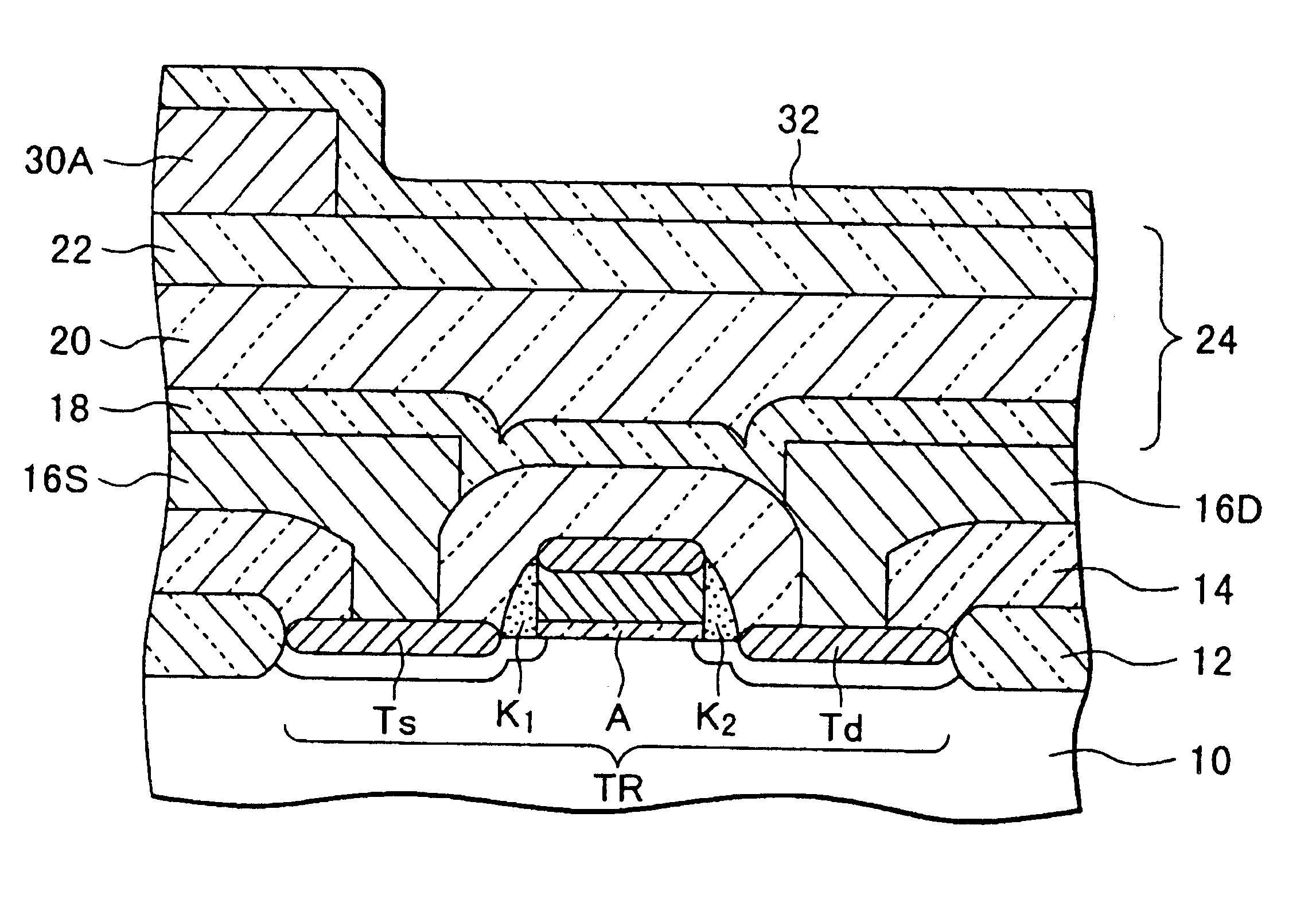
Figure 1 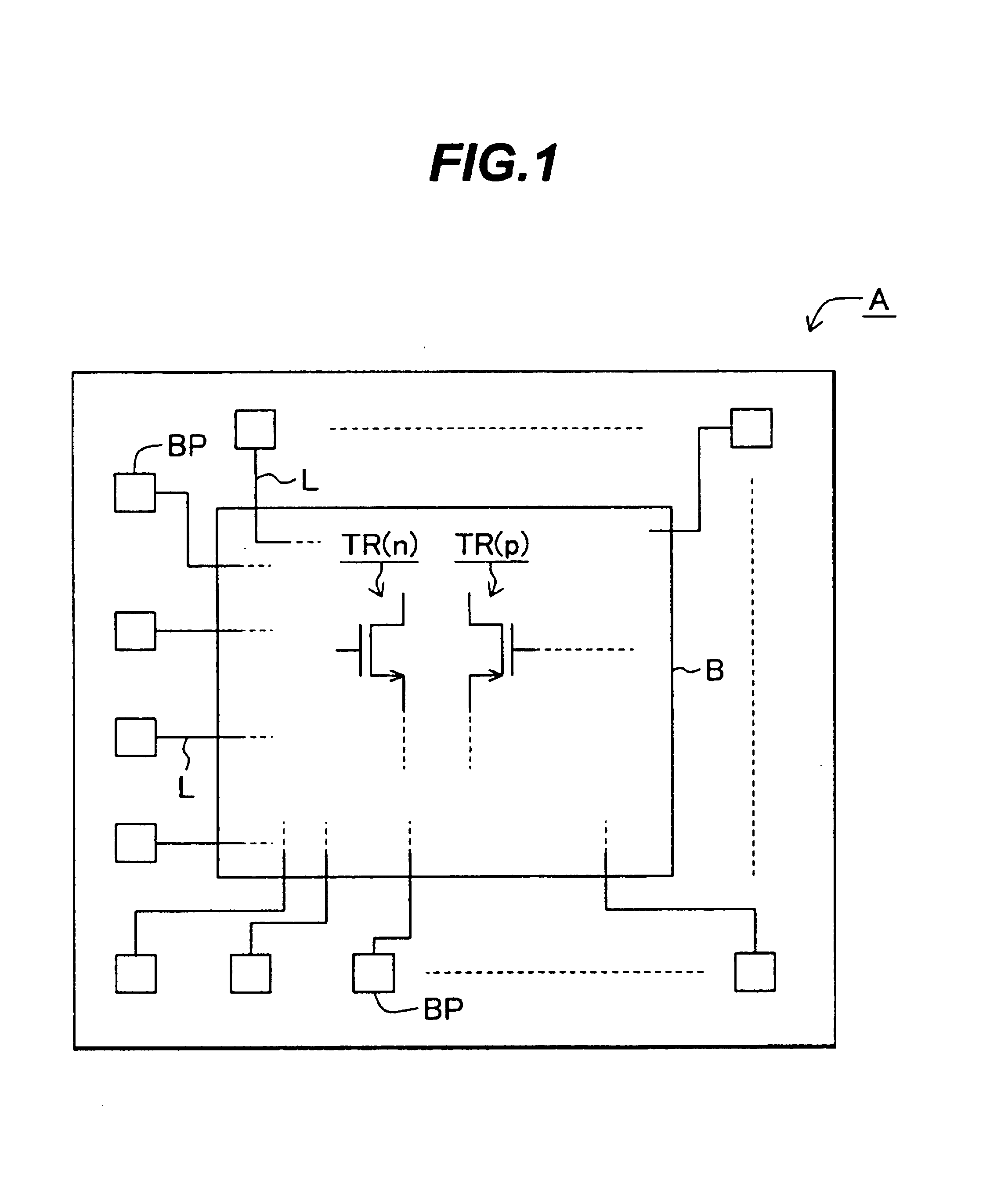
Figure 2 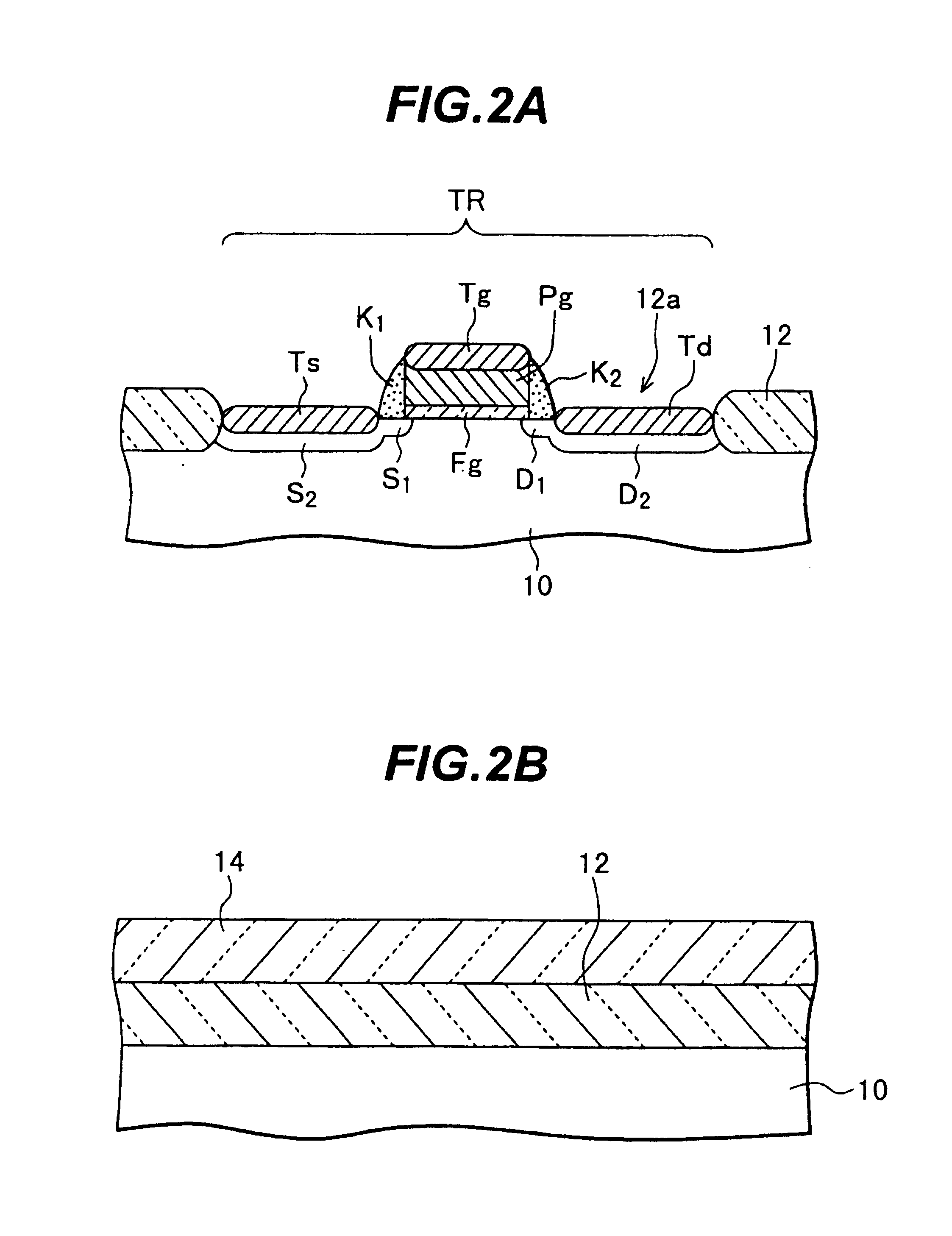
Figure 3
Abstract
Description
[0001] This application is based on Japanese Patent Application HEI 11-055341 filed on Mar. 3, 1999, all the contents of which are incorporated herein by reference.BACKGROUND OF THE INVENTION
[0002] a) Field of the Invention
[0003] The present invention relates to a method of manufacturing a semiconductor device with MOS transistors (insulated gate type field effect transistors), and more particularly to techniques capable of easily lowering a variation in threshold voltages of MOS transistors by forming a wiring layer on an interlayer insulating film including a hydrogen containing film, forming a silicon nitride film as a surface protection film (passivation film) on the wiring layer, and thereafter performing heat treatment to lower interface state density.
[0004] b) Description of the Related Art
[0005] In a semiconductor device having a surface protection film, for example, as shown in FIG. 6, on the surface of an interlayer insulating film 1, wiring layers 2A and 2B near to each other ...
Examples
Embodiment Construction
[0041]A MOS type IC manufacture method according to an embodiment of the invention will be described with reference to FIG. 1, FIGS. 2A to 2I and FIG. 3.
[0042]FIG. 1 is a schematic plan view of a MOS type IC. As shown in FIG. 1, a MOS type IC A has an integrated circuit area B formed with an integrated circuit, and a number of bonding pads BP disposed around the integrated circuit area B. The integrated circuit in the integrated circuit area B has a number of MOS transistors. A CMOS type IC is made of basic CMOS circuits each constituted of pairs of one n-channel MOS transistor TR(n) and one p-channel MOS transistor TR(p). Transistors, CMOS circuits and bonding pads BP are electrically connected by wiring patterns L.
[0043]Next, a manufacture method for a CMOS circuit will be described. As shown in FIG. 2A, on the surface of a semiconductor substrate 10 made of, for example, silicon, a field insulating film (silicon oxide film) 12 defining an active region 12a is formed by LOCOS. For...