Analysis of Semiconductor Materials in Photonic Integrated Circuits
SEP 29, 20259 MIN READ
Generate Your Research Report Instantly with AI Agent
Patsnap Eureka helps you evaluate technical feasibility & market potential.
Photonic IC Semiconductor Materials Background and Objectives
Photonic Integrated Circuits (PICs) represent a revolutionary advancement in semiconductor technology, merging optical and electronic functionalities on a single chip. The evolution of semiconductor materials for PICs traces back to the 1980s, beginning with III-V compound semiconductors like Gallium Arsenide (GaAs) and Indium Phosphide (InP). These materials initially enabled basic photonic components such as waveguides and modulators, laying the foundation for integrated photonics.
The technological trajectory has since expanded to include Silicon (Si), Silicon-on-Insulator (SOI), Silicon Nitride (Si3N4), and more recently, emerging materials like Lithium Niobate (LiNbO3) and various two-dimensional materials. Each material system offers distinct advantages in terms of optical properties, integration capabilities, and manufacturing compatibility, driving the diversification of PIC platforms to address specific application requirements.
Current trends in semiconductor materials for PICs are moving toward heterogeneous integration, combining the strengths of different material platforms to overcome individual limitations. This approach aims to leverage the mature CMOS fabrication infrastructure of silicon photonics while incorporating the superior light emission capabilities of III-V materials, creating hybrid solutions that maximize performance and functionality.
The primary technical objectives in this field include achieving higher levels of integration density, reducing optical losses at material interfaces, enhancing modulation efficiency, and improving thermal stability across operating conditions. Additionally, there is significant focus on developing materials that enable broader wavelength operation, from visible to mid-infrared ranges, to expand the application scope of PICs.
From a manufacturing perspective, key objectives include developing scalable fabrication processes compatible with existing semiconductor manufacturing infrastructure, reducing production costs, and improving yield rates for complex photonic structures. The industry is particularly focused on standardization efforts to establish common design rules, process parameters, and testing methodologies.
Looking forward, the field aims to develop novel semiconductor materials and structures that can support emerging quantum photonic applications, neuromorphic computing, and ultra-high-speed optical communications beyond 1 Tb/s. Research is increasingly directed toward materials that can facilitate programmable photonics, where optical properties can be dynamically reconfigured post-fabrication, enabling more versatile and adaptive photonic systems.
The convergence of these technological developments is expected to drive PICs toward unprecedented levels of functionality and performance, potentially revolutionizing fields ranging from telecommunications and data centers to biomedical sensing and quantum information processing.
Market Analysis for Photonic Integrated Circuits
The global market for Photonic Integrated Circuits (PICs) is experiencing robust growth, driven by increasing demand for high-speed data transmission, telecommunications infrastructure expansion, and emerging applications in quantum computing. Current market valuations place the PIC sector at approximately 1.3 billion USD in 2023, with projections indicating a compound annual growth rate (CAGR) of 23% through 2030, potentially reaching 5.5 billion USD by the end of the decade.
Telecommunications remains the dominant application segment, accounting for nearly 40% of the total market share. This is primarily due to the critical role PICs play in fiber optic networks, coherent optical systems, and next-generation 5G/6G infrastructure. Data centers represent the fastest-growing segment with a 28% annual growth rate, as hyperscale providers increasingly adopt PIC-based transceivers to manage exponential bandwidth demands.
Regionally, North America currently leads the market with approximately 35% share, followed by Asia-Pacific at 32% and Europe at 25%. However, the Asia-Pacific region, particularly China, Taiwan, and Singapore, is expected to demonstrate the highest growth trajectory over the next five years due to substantial investments in domestic semiconductor manufacturing capabilities and optical communication networks.
Consumer demand patterns reveal increasing preference for smaller form factors, lower power consumption, and higher integration density in photonic components. This trend aligns with the broader industry movement toward sustainable technologies, as PICs typically consume 30-50% less power than traditional electronic integrated circuits for equivalent data processing tasks.
Market segmentation by material platform shows silicon photonics dominating with approximately 45% market share, followed by indium phosphide (InP) at 30% and silicon nitride platforms at 15%. The remaining 10% comprises emerging materials including lithium niobate, polymers, and glass. Silicon photonics maintains its lead due to compatibility with CMOS manufacturing infrastructure, while InP offers superior performance for active photonic components.
Key market drivers include the exponential growth in global data traffic (increasing at 26% annually), the transition to 400G/800G optical networks, and emerging applications in automotive LiDAR, biosensing, and quantum technologies. Restraining factors include high initial manufacturing costs, packaging challenges, and technical limitations in achieving full integration of all optical functions on a single chip.
The competitive landscape features both established telecommunications equipment manufacturers and specialized photonics startups, with increasing vertical integration as larger companies acquire specialized technology providers to secure strategic advantages in the rapidly evolving ecosystem.
Current Status and Challenges in PIC Semiconductor Materials
Photonic Integrated Circuits (PICs) have emerged as a transformative technology in the semiconductor industry, with global research efforts intensifying over the past decade. Currently, the field employs several semiconductor material platforms, each with distinct advantages and limitations that shape their application domains.
Silicon photonics dominates the commercial landscape, leveraging existing CMOS infrastructure and offering cost-effective manufacturing at scale. However, silicon's indirect bandgap presents fundamental challenges for light emission, necessitating hybrid integration approaches with III-V materials. Recent advancements in germanium-on-silicon and silicon-germanium alloys have partially addressed these limitations, though efficiency remains suboptimal compared to direct bandgap alternatives.
III-V compound semiconductors, particularly indium phosphide (InP) and gallium arsenide (GaAs), represent the gold standard for active photonic components due to their direct bandgap properties. These materials excel in light generation and amplification but face integration challenges with silicon-based electronic circuits. Current fabrication processes for III-V PICs remain costly and less mature than silicon counterparts, with wafer sizes typically limited to 3-4 inches compared to silicon's 12-inch standard.
Silicon nitride has emerged as a promising middle-ground platform, offering lower propagation losses than silicon and broader operational wavelength ranges. Its CMOS compatibility enables relatively straightforward integration, though it shares silicon's limitations regarding active components. Recent developments in ultra-low-loss silicon nitride waveguides have achieved propagation losses below 0.1 dB/cm, enabling new applications in quantum photonics and sensing.
Lithium niobate on insulator (LNOI) represents another significant advancement, offering exceptional electro-optic properties for high-speed modulators. However, manufacturing challenges and material costs have limited widespread adoption despite its superior performance characteristics.
A critical challenge across all material platforms remains the efficient integration of different semiconductor materials to leverage their complementary strengths. Current approaches include direct epitaxial growth, wafer bonding, and transfer printing, each presenting trade-offs between alignment precision, thermal compatibility, and manufacturing complexity.
Scaling production while maintaining performance consistency represents another significant hurdle. Variations in material properties and processing conditions can lead to device performance inconsistencies, particularly problematic for applications requiring precise wavelength control such as WDM systems.
The environmental stability of PIC materials also presents ongoing challenges, with temperature sensitivity affecting wavelength stability and device performance. Current compensation techniques add complexity and power requirements to PIC systems, limiting their deployment in harsh environments.
Current Semiconductor Material Solutions for PICs
01 Semiconductor material fabrication and processing
Various methods and techniques for fabricating and processing semiconductor materials, including deposition, etching, and surface treatment processes. These techniques are essential for creating semiconductor devices with specific electrical properties and performance characteristics. The processes may involve chemical vapor deposition, physical vapor deposition, or other specialized methods to create high-quality semiconductor layers.- Semiconductor material fabrication and processing: Various methods and techniques for fabricating and processing semiconductor materials, including deposition, etching, and surface treatment processes. These techniques are essential for creating high-quality semiconductor materials with specific electrical properties for use in electronic devices. The processes may involve chemical vapor deposition, physical vapor deposition, or other specialized techniques to achieve desired material characteristics.
- Novel semiconductor material compositions: Development of new semiconductor material compositions with enhanced properties, such as improved conductivity, thermal stability, or optical characteristics. These novel materials may include compound semiconductors, alloys, or doped materials designed to meet specific performance requirements for advanced electronic applications. The compositions are engineered at the molecular level to achieve desired band gaps and carrier mobility.
- Semiconductor testing and characterization methods: Methods and systems for testing and characterizing semiconductor materials to determine their electrical, optical, and structural properties. These techniques include various analytical methods such as spectroscopy, microscopy, and electrical measurements to evaluate material quality and performance. Accurate characterization is crucial for quality control in semiconductor manufacturing and for research and development of new materials.
- Semiconductor materials for specific applications: Specialized semiconductor materials designed for specific applications such as photovoltaics, light-emitting diodes, sensors, or power electronics. These materials are tailored to meet the unique requirements of each application, such as bandgap engineering for solar cells or high electron mobility for high-frequency devices. The selection and optimization of semiconductor materials significantly impact device performance and efficiency.
- Semiconductor material handling and packaging: Technologies related to the handling, storage, and packaging of semiconductor materials to maintain their integrity and prevent contamination. This includes specialized containers, transport systems, and environmental controls designed to protect sensitive semiconductor materials throughout the supply chain and manufacturing process. Proper handling is essential to prevent defects and ensure the reliability of finished semiconductor devices.
02 Novel semiconductor material compositions
Development of new semiconductor material compositions with enhanced properties, such as improved conductivity, thermal stability, or optical characteristics. These materials may include compound semiconductors, alloys, or doped materials designed for specific applications in electronics, optoelectronics, or energy conversion. The compositions are engineered at the molecular level to achieve desired band gaps and carrier mobility.Expand Specific Solutions03 Semiconductor testing and quality control
Methods and systems for testing and evaluating semiconductor materials to ensure quality and performance. These include techniques for measuring electrical properties, detecting defects, and characterizing material composition. Advanced analytical tools such as spectroscopy, microscopy, and electrical testing are employed to verify that semiconductor materials meet specifications before device fabrication.Expand Specific Solutions04 Semiconductor materials for specific applications
Specialized semiconductor materials designed for particular applications such as photovoltaics, sensors, light-emitting diodes, or high-power electronics. These materials are tailored with specific properties to optimize performance in their intended application domains. The composition and structure of these materials are engineered to enhance specific characteristics such as light absorption, emission wavelength, or power handling capability.Expand Specific Solutions05 Semiconductor material handling and packaging
Technologies for handling, storing, and packaging semiconductor materials to prevent contamination and damage during manufacturing processes. This includes specialized containers, transport mechanisms, and environmental controls to maintain material integrity. Proper handling is critical to prevent defects and ensure the reliability of finished semiconductor devices.Expand Specific Solutions
Key Industry Players in Photonic Integration
The semiconductor materials market for Photonic Integrated Circuits (PICs) is currently in a growth phase, with an expanding competitive landscape characterized by both established players and innovative startups. Major corporations like Intel, Samsung, and GlobalFoundries are leveraging their semiconductor manufacturing expertise to develop advanced PIC solutions, while specialized companies such as Skorpios Technologies, SMART Photonics, and EFFECT Photonics are driving innovation through fabless and foundry business models. The technology is approaching maturity in telecommunications applications but remains emerging in areas like quantum computing and biosensing. Research institutions including IMEC, Cornell University, and Chinese Academy of Sciences are accelerating development through academic-industrial partnerships, pushing material innovations in silicon photonics, III-V semiconductors, and hybrid integration platforms.
Intel Corp.
Technical Solution: Intel has developed a comprehensive silicon photonics platform that integrates III-V materials with silicon to create high-performance photonic integrated circuits (PICs). Their technology utilizes hybrid silicon lasers where InP-based gain materials are bonded to silicon waveguides, enabling efficient light generation while leveraging silicon's processing advantages. Intel's 400G photonic integrated circuits employ four wavelength channels at 100 Gbps each, utilizing advanced modulation schemes. Their manufacturing approach incorporates standard CMOS processes with specialized III-V integration techniques, allowing for wafer-scale production of photonic components alongside electronic elements. Intel has demonstrated data transmission rates exceeding 400 Gbps with their silicon photonics technology, with roadmaps targeting terabit-per-second capabilities for next-generation data centers and high-performance computing applications.
Strengths: Leverages existing CMOS manufacturing infrastructure; achieves high integration density of photonic and electronic components; demonstrates excellent scalability for mass production. Weaknesses: Hybrid integration techniques add manufacturing complexity; thermal management challenges at high data rates; higher cost compared to pure electronic solutions.
AMS OSRAM INTERNATIONAL GMBH
Technical Solution: AMS OSRAM has pioneered advanced semiconductor materials for photonic integrated circuits focusing on specialized compound semiconductors. Their technology platform utilizes III-V materials including GaAs, InP, and GaN to create high-performance light sources and detectors for PICs. The company has developed proprietary epitaxial growth processes that enable precise control of semiconductor layer structures at the atomic level, crucial for optimizing optical properties. Their vertical-cavity surface-emitting laser (VCSEL) technology incorporates sophisticated distributed Bragg reflector structures with quantum well active regions, achieving high efficiency and spectral purity. For sensing applications, AMS OSRAM has developed integrated photodetector arrays using specialized semiconductor materials that provide enhanced sensitivity across specific wavelength ranges. Their manufacturing approach combines wafer-level processing with advanced packaging techniques to create miniaturized photonic components for applications ranging from consumer electronics to automotive LiDAR systems.
Strengths: Exceptional expertise in compound semiconductor materials; vertical integration from material development to device manufacturing; specialized optimization for specific wavelengths and applications. Weaknesses: Higher production costs compared to silicon-based solutions; more complex manufacturing processes; challenges in achieving the same level of integration density as silicon photonics.
Critical Patents and Innovations in PIC Materials
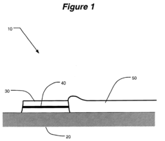
Photonic integrated circuit (PIC) and method for making same
PatentInactiveUS6788721B2
Innovation
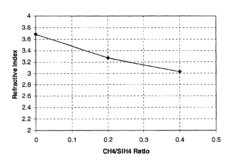
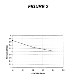
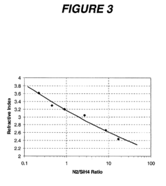
- The use of amorphous silicon (a-Si) materials, such as a-Si:H and a-Si:F based alloys, for waveguide formation in PICs, allowing for flexible index matching and low-loss coupling between active and passive components, achieved through Plasma Enhanced Chemical Vapor Deposition (PECVD) processes, which eliminates lattice match requirements and reduces optical absorption.
Photonic integrated circuit packages including substrates with glass cores
PatentPendingUS20240178207A1
Innovation
- The use of a glass interposer with through-glass vias (TGVs) and optical pathways allows for high-density interconnects between PICs and optical components, minimizing z-height offset by optically coupling PICs through the interposer and electrically coupling them via TGVs with hybrid bonds, enabling efficient optical and electrical connectivity.
Manufacturing Processes and Fabrication Techniques
The manufacturing processes for photonic integrated circuits (PICs) involve sophisticated techniques adapted from traditional semiconductor fabrication, yet with unique requirements specific to photonic applications. The primary fabrication approach employs epitaxial growth methods, with Molecular Beam Epitaxy (MBE) and Metal-Organic Chemical Vapor Deposition (MOCVD) being the dominant techniques for creating precise semiconductor layers with controlled optical properties.
MOCVD offers higher throughput and has become the industry standard for III-V compound semiconductor deposition, particularly for InP and GaAs-based photonic devices. This process enables the creation of quantum wells and other nanostructures critical for active photonic components such as lasers and modulators, with atomic-level precision in layer thickness and composition.
Lithography represents another crucial fabrication step, with deep-UV lithography (193nm) currently being the mainstream technique for silicon photonics. However, electron-beam lithography remains essential for research environments and specialized applications requiring sub-100nm features. The industry is gradually transitioning toward immersion lithography and exploring next-generation techniques like nanoimprint lithography to achieve higher resolution while maintaining cost-effectiveness.
Etching processes present unique challenges in PIC fabrication due to the requirement for vertical sidewalls and minimal surface roughness to reduce optical scattering losses. Reactive Ion Etching (RIE) and Inductively Coupled Plasma (ICP) etching have been optimized with specialized chemistries for different semiconductor materials, with particular attention to achieving smooth waveguide surfaces.
Integration of different materials presents significant manufacturing challenges. Heterogeneous integration approaches include wafer bonding techniques, particularly direct bonding and adhesive bonding, which have enabled the combination of III-V gain materials with silicon photonic circuits. Recent advances in selective area growth and epitaxial regrowth have shown promise for monolithic integration of different functionalities.
Packaging remains one of the most cost-intensive aspects of PIC manufacturing, accounting for up to 80% of device costs in some applications. Fiber-to-chip coupling techniques have evolved from edge coupling to grating couplers, with ongoing research focused on reducing coupling losses and increasing alignment tolerances. Automated active alignment systems have significantly improved manufacturing throughput, though passive alignment techniques are being developed to further reduce costs.
The yield management for PICs requires specialized testing protocols, including on-wafer optical probing and automated visual inspection systems capable of detecting sub-micron defects that can impact optical performance. Recent developments in machine learning-based defect classification have improved detection rates and reduced false positives in the manufacturing process.
Environmental Impact and Sustainability Considerations
The semiconductor materials used in photonic integrated circuits (PICs) present significant environmental challenges throughout their lifecycle. The extraction of rare earth elements and high-purity silicon requires extensive mining operations that contribute to habitat destruction, soil erosion, and water pollution. Manufacturing processes for III-V compound semiconductors like gallium arsenide and indium phosphide involve toxic substances that pose serious environmental and health risks if not properly managed.
Energy consumption represents another critical environmental concern in PIC production. The fabrication of semiconductor materials demands extremely high temperatures and ultra-clean environments, resulting in substantial carbon footprints. Current estimates suggest that the energy required to produce a single semiconductor wafer can exceed several megawatt-hours, with corresponding greenhouse gas emissions contributing to climate change impacts.
Water usage in semiconductor manufacturing is particularly problematic, with a typical fabrication facility consuming millions of gallons daily for cleaning and processing. This intensive water consumption becomes increasingly unsustainable in regions facing water scarcity, creating potential conflicts between industrial and community needs.
End-of-life considerations for PIC components present additional challenges. Many semiconductor materials contain elements that are difficult to recycle and potentially hazardous if improperly disposed of. The current recycling rate for these specialized materials remains disappointingly low, with most decommissioned photonic components ending up in landfills.
The industry has begun implementing sustainability initiatives to address these concerns. Leading manufacturers are investing in closed-loop water systems that can reduce freshwater consumption by up to 90%. Energy efficiency improvements through optimized clean room designs and more efficient equipment have demonstrated potential to reduce carbon emissions by 30-40% in newer fabrication facilities.
Material innovation represents a promising path toward sustainability. Research into silicon photonics offers environmental advantages over III-V compounds, while emerging bio-based semiconductor materials could potentially reduce dependence on environmentally problematic mining operations. Additionally, design for recyclability approaches are gaining traction, with modular PIC designs that facilitate component recovery and reuse.
Regulatory frameworks are evolving globally to address the environmental impacts of semiconductor manufacturing. The European Union's Restriction of Hazardous Substances (RoHS) directive and similar regulations in other regions are driving the industry toward greener materials and processes, though significant gaps in oversight remain in many developing economies where manufacturing is increasingly concentrated.
Unlock deeper insights with Patsnap Eureka Quick Research — get a full tech report to explore trends and direct your research. Try now!
Generate Your Research Report Instantly with AI Agent
Supercharge your innovation with Patsnap Eureka AI Agent Platform!