Assessing the Role of EUV Lithography in Integrated Circuit Fabrication
OCT 14, 20259 MIN READ
Generate Your Research Report Instantly with AI Agent
Patsnap Eureka helps you evaluate technical feasibility & market potential.
EUV Lithography Evolution and Objectives
Extreme Ultraviolet (EUV) lithography represents a revolutionary advancement in semiconductor manufacturing technology, emerging after decades of research and development efforts. The evolution of this technology can be traced back to the 1980s when researchers began exploring alternative lithography methods to overcome the physical limitations of traditional optical lithography. By the late 1990s, EUV was identified as a promising candidate for next-generation lithography, capable of achieving feature sizes below 10nm.
The technological progression of EUV lithography has been marked by significant milestones. Initially, researchers faced fundamental challenges in developing suitable light sources, mirrors, and photoresist materials compatible with the 13.5nm wavelength used in EUV. The period between 2000 and 2010 saw intensive research focused on these core components, with breakthroughs in laser-produced plasma (LPP) sources and multilayer mirror technology.
From 2010 to 2017, the industry witnessed the transition from laboratory research to industrial implementation, with companies like ASML developing the first commercial EUV lithography systems. The introduction of ASML's NXE series marked a turning point, demonstrating the feasibility of EUV technology in high-volume manufacturing environments. By 2019, leading semiconductor manufacturers began incorporating EUV lithography into their production processes for advanced nodes.
The primary objective of EUV lithography is to enable the continuation of Moore's Law by facilitating the production of increasingly smaller transistors and more complex integrated circuits. Specifically, EUV aims to achieve reliable patterning of features below 7nm while maintaining economic viability in high-volume manufacturing scenarios. This technology seeks to reduce the complexity of multi-patterning techniques required with previous lithography methods.
Another critical goal is improving production efficiency. EUV lithography aims to simplify the manufacturing process by reducing the number of process steps required for complex patterns, potentially lowering production costs and time-to-market for advanced semiconductor devices. This simplification becomes increasingly important as circuit designs grow more intricate.
Looking forward, the technology roadmap for EUV lithography includes objectives for enhancing system throughput, currently a limiting factor in widespread adoption. Research efforts are focused on increasing source power, improving photoresist sensitivity, and optimizing overall system efficiency to achieve economically viable production rates exceeding 100-125 wafers per hour.
Additionally, the industry is exploring high-numerical-aperture (high-NA) EUV systems as the next evolution, aiming to extend the technology's capabilities to the 3nm node and beyond. This advancement represents the continued trajectory of EUV technology in supporting the semiconductor industry's relentless pursuit of higher performance and greater functionality in integrated circuits.
Semiconductor Industry Demand Analysis
The semiconductor industry's demand for advanced lithography technologies, particularly EUV (Extreme Ultraviolet) lithography, is driven by the relentless pursuit of Moore's Law and the economic imperatives of chip manufacturing. Market analysis indicates that the global semiconductor industry reached $573 billion in 2022, with projections to exceed $1 trillion by 2030, creating substantial demand for next-generation fabrication technologies.
EUV lithography addresses a critical market need as traditional DUV (Deep Ultraviolet) lithography approaches its physical limits at advanced nodes. The industry demand is particularly acute in the sub-7nm process technology space, where multiple patterning techniques with DUV become economically prohibitive due to increased process steps, yield challenges, and time-to-market delays.
Leading semiconductor manufacturers including TSMC, Samsung, and Intel have committed substantial capital expenditure toward EUV implementation, with TSMC alone investing over $20 billion in advanced fabrication facilities incorporating EUV technology. This investment trend reflects the market's recognition that EUV is essential for maintaining competitive manufacturing capabilities at 5nm nodes and beyond.
Consumer electronics, particularly smartphones and high-performance computing applications, represent the primary demand drivers for EUV-enabled chips. The smartphone market, valued at approximately $522 billion, continues to demand increasingly powerful processors in smaller form factors, directly benefiting from the node shrinkage that EUV enables.
The automotive semiconductor segment presents another significant growth vector, with projections indicating a 12% CAGR through 2028 as vehicles incorporate more advanced driver assistance systems and autonomous capabilities requiring sophisticated processors manufactured at advanced nodes.
Cloud computing and data center applications constitute a third major demand segment, with hyperscalers continuously seeking more energy-efficient chips to manage exponentially growing data processing requirements while controlling operational costs. This efficiency imperative directly translates to demand for the most advanced process nodes that EUV enables.
Geographic analysis reveals that East Asia dominates the demand landscape, with Taiwan, South Korea, and increasingly China representing the largest markets for EUV equipment. North America follows, driven primarily by Intel's renewed manufacturing focus and various government initiatives to strengthen domestic semiconductor production capabilities.
The industry's willingness to absorb the significant cost premium of EUV lithography—with each EUV scanner priced at approximately $150 million—underscores the critical market need for this technology in maintaining competitive manufacturing capabilities and meeting end-market demands for higher performance, lower power consumption, and increased functionality in semiconductor devices.
EUV Technology Status and Barriers
Extreme Ultraviolet (EUV) lithography represents a revolutionary advancement in semiconductor manufacturing, operating at a wavelength of 13.5nm. This technology has progressed from theoretical concept to commercial implementation over the past two decades, with ASML emerging as the dominant equipment supplier. Despite significant progress, EUV technology faces substantial technical barriers that impact its widespread adoption across the semiconductor industry.
The current global landscape shows uneven distribution of EUV capabilities, with advanced semiconductor manufacturing nations like Taiwan, South Korea, and the United States leading implementation. Europe maintains strong research capabilities while China faces significant access restrictions due to export controls. This geographic disparity creates strategic implications for semiconductor supply chains and national technology policies.
From a technical perspective, EUV systems currently operate at approximately 250 watts of source power, enabling production throughput of around 160 wafers per hour. While this represents remarkable progress, it remains below the ideal target of 500 watts needed for optimal economic efficiency. The complexity of generating and controlling EUV light creates fundamental physical challenges that continue to constrain performance improvements.
Power source limitations represent a primary barrier, as generating sufficient EUV photons requires creating tin plasma at temperatures exceeding 500,000°C through laser pulses. The resulting debris management, mirror degradation, and thermal load issues create significant engineering challenges. Current systems experience approximately 5-10% reflectivity loss in collector mirrors over operational lifetimes, necessitating costly maintenance cycles.
Photoresist technology presents another critical challenge. EUV photons carry significantly more energy than traditional deep ultraviolet (DUV) light, creating complex photochemical reactions that impact pattern resolution and line edge roughness. Current EUV resists struggle to simultaneously achieve high sensitivity, low line edge roughness, and minimal pattern collapse at sub-7nm nodes.
Mask defectivity remains problematic despite advances in inspection tools. Unlike transparent masks used in DUV lithography, EUV employs reflective masks with complex multilayer structures. Defects in these structures can cause pattern distortions that are difficult to detect and repair. Current defect detection capabilities remain insufficient for the most advanced nodes, with particular challenges in identifying buried defects within multilayer structures.
Stochastic effects represent perhaps the most fundamental barrier to EUV scaling. At extreme dimensions, random variations in photon absorption, secondary electron generation, and chemical reactions create statistical uncertainties that manifest as yield-limiting defects. These effects become increasingly pronounced below 20nm pitch, threatening the economic viability of future technology nodes without significant innovations in materials and process control.
Current EUV Implementation Approaches
01 EUV lithography system design and components
EUV lithography systems incorporate specialized components designed to work with extreme ultraviolet light. These systems typically include radiation sources, optical elements, and positioning mechanisms that enable precise pattern transfer at nanometer scales. The design focuses on managing the unique properties of EUV radiation, including its absorption characteristics and interaction with various materials, to achieve high-resolution semiconductor manufacturing.- EUV lithography system components and design: EUV lithography systems incorporate specialized components designed for extreme ultraviolet wavelengths. These systems typically include reflective optics, specialized light sources, and vacuum environments to enable high-resolution patterning. The design focuses on achieving optimal imaging performance while addressing challenges related to EUV light absorption and reflection properties.
- EUV light source technology: EUV lithography requires specialized light sources capable of generating extreme ultraviolet radiation at specific wavelengths (typically 13.5nm). These sources often utilize laser-produced plasma or discharge-produced plasma technologies where high-energy lasers or electrical discharges strike target materials to generate EUV photons. Innovations focus on increasing source power, stability, and conversion efficiency while reducing debris generation.
- EUV mask and reticle technology: EUV lithography employs reflective masks rather than traditional transmissive photomasks. These masks consist of multilayer reflective coatings with absorber patterns on top. Innovations in this area focus on defect mitigation, pattern accuracy, and reflectivity optimization. Advanced inspection and repair techniques are developed to ensure mask quality meets the stringent requirements of EUV lithography.
- EUV resist materials and processing: Specialized photoresist materials are developed for EUV lithography to achieve high sensitivity, resolution, and pattern fidelity with the lower photon flux of EUV radiation. These materials must balance sensitivity, line edge roughness, and resolution while being compatible with existing semiconductor manufacturing processes. Innovations include chemical amplification mechanisms, metal-containing resists, and novel development processes.
- EUV lithography process control and optimization: Advanced process control techniques are essential for EUV lithography to maintain consistent patterning results. This includes sophisticated metrology systems, computational lithography approaches, and feedback mechanisms to compensate for process variations. Innovations focus on overlay accuracy, critical dimension uniformity, and defect detection to enable high-volume manufacturing with EUV technology.
02 Contamination control and mitigation in EUV systems
Contamination control is critical in EUV lithography due to the sensitivity of optical components to molecular and particulate contamination. Various techniques are employed to prevent, detect, and remove contaminants that can degrade system performance. These include specialized cleaning methods, protective coatings for optical surfaces, and environmental control systems that maintain ultra-clean conditions within the lithography equipment.Expand Specific Solutions03 EUV mask technology and inspection
EUV masks require specialized materials and structures to effectively pattern EUV radiation. These masks typically employ reflective rather than transmissive designs and incorporate multiple layers to enhance reflectivity at EUV wavelengths. Advanced inspection and repair technologies are essential for detecting and addressing defects in these masks, as even nanoscale imperfections can cause critical pattern failures in the manufactured semiconductor devices.Expand Specific Solutions04 Thermal management in EUV lithography
Thermal management is a significant challenge in EUV lithography systems due to the high energy levels involved. The absorption of EUV radiation generates substantial heat that can cause thermal expansion, distortion, and damage to sensitive components. Advanced cooling systems, thermally stable materials, and compensation mechanisms are employed to maintain dimensional stability and ensure consistent imaging performance under varying thermal conditions.Expand Specific Solutions05 EUV source technology and optimization
EUV radiation sources represent a critical component of lithography systems, typically based on laser-produced plasma or discharge-produced plasma technologies. These sources must generate sufficient power at the required wavelength while maintaining stability over extended operation periods. Ongoing development focuses on increasing source power, improving conversion efficiency, reducing debris generation, and extending component lifetimes to enhance overall system productivity and reduce operational costs.Expand Specific Solutions
EUV Equipment Manufacturers and Ecosystem
EUV lithography in integrated circuit fabrication is currently in a growth phase, with the market expected to expand significantly due to increasing demand for advanced semiconductor nodes. The technology has reached commercial maturity but continues to evolve rapidly. Leading players include ASML Netherlands BV as the dominant EUV equipment supplier, while semiconductor manufacturers Taiwan Semiconductor Manufacturing Co. (TSMC), Samsung Electronics, and Intel are driving adoption. GlobalFoundries and United Microelectronics Corporation (UMC) are also investing in EUV capabilities. The competitive landscape features collaboration between equipment suppliers like Applied Materials and semiconductor manufacturers, with research institutions such as the Institute of Microelectronics of Chinese Academy of Sciences contributing to technological advancement. The high capital requirements create significant barriers to entry, consolidating market power among established players.
Taiwan Semiconductor Manufacturing Co., Ltd.
Technical Solution: TSMC has pioneered the implementation of EUV lithography in high-volume manufacturing, beginning with their 7nm+ process node and expanding to their 5nm and 3nm technologies. Their approach involves a comprehensive EUV integration strategy that includes specialized photoresist materials, optimized mask technologies, and advanced computational lithography techniques. TSMC's EUV implementation enables printing features as small as 13nm half-pitch with single exposure techniques [1]. The company has invested over $17 billion in EUV infrastructure and currently operates more than 50 ASML EUV systems across their global fabrication facilities [2]. Their EUV process achieves greater than 90% availability and productivity exceeding 125 wafers per hour in production environments. TSMC has developed proprietary computational correction techniques to address stochastic effects and pattern fidelity challenges inherent to EUV lithography, resulting in defect densities below 0.1/cm² for critical layers [3].
Strengths: Industry-leading EUV implementation with highest wafer throughput and yield rates; extensive experience across multiple process nodes; proprietary computational correction techniques. Weaknesses: Extremely high capital costs for EUV equipment and facility requirements; dependency on ASML as sole EUV equipment supplier; challenges with EUV mask infrastructure and inspection.
Intel Corp.
Technical Solution: Intel has developed a multi-faceted approach to EUV lithography implementation, focusing on both hardware and process innovations. Their strategy includes the development of specialized photoresists with enhanced sensitivity and reduced line edge roughness, achieving 30% improvement in critical dimension uniformity compared to earlier generations [1]. Intel's EUV implementation incorporates advanced computational lithography techniques, including source-mask optimization and inverse lithography technology, which enable more precise pattern transfer. The company has invested approximately $5 billion in EUV infrastructure across their fabrication network and has deployed EUV lithography in their 7nm (Intel 4) process and beyond [2]. Intel's approach includes innovative pellicle designs that improve transmission efficiency to over 88% while maintaining thermal stability under high-power EUV exposure. Their EUV process achieves defect densities below 0.15/cm² and supports high-volume manufacturing with system availability exceeding 85% [3]. Intel has also pioneered the use of high-numerical aperture (High-NA) EUV technology in partnership with ASML, preparing for future nodes below 3nm.
Strengths: Comprehensive in-house research capabilities; vertical integration allowing for customized EUV solutions; early adoption of High-NA EUV technology for future nodes. Weaknesses: Delayed implementation compared to competitors like TSMC; higher initial defect densities during ramp-up; challenges in achieving cost-effective implementation across multiple fabs globally.
Critical EUV Patents and Technical Innovations
Methods for optical proximity correction in the design and fabrication of integrated circuits using extreme ultraviolet lithography
PatentActiveUS9651855B2
Innovation
- The implementation of novel optical proximity correction (OPC) techniques that generate a third polygon with dimensions corresponding to the combination of first and second design polygons and a filled polygon within it, allowing for closer tip proximity without the need for multiple masks.
Extreme ultraviolet mirrors and masks with improved reflectivity
PatentInactiveUS20180226166A1
Innovation
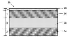
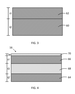
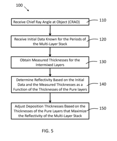
- A method to optimize the reflectivity of multi-layer stacks in EUV optical elements by determining and selecting the thicknesses of intermixed and pure layers to maximize reflectivity, using a computer-based system that considers intermixing and deposition conditions, and implementing these optimizations in Bragg mirrors and masks.
Economic Impact of EUV Adoption
The adoption of Extreme Ultraviolet (EUV) lithography represents a significant economic inflection point for the semiconductor industry. Initial capital investments for EUV technology are substantial, with each lithography system costing approximately $120-150 million, compared to $40-60 million for traditional deep ultraviolet (DUV) systems. This steep entry barrier has created a tiered semiconductor manufacturing landscape, where only the largest foundries like TSMC, Samsung, and Intel can afford full-scale EUV implementation.
Despite these high upfront costs, the economic benefits of EUV adoption become apparent in high-volume manufacturing scenarios. Process simplification represents a major cost advantage, as EUV can replace multiple DUV lithography steps with a single exposure. For advanced nodes below 7nm, this reduction in process steps translates to approximately 20-30% lower production costs per wafer once the technology reaches maturity and economies of scale.
The economic ripple effects extend throughout the semiconductor supply chain. Equipment suppliers like ASML have experienced significant revenue growth, with their EUV business segment growing at over 35% annually since 2018. Material suppliers specializing in EUV-specific photoresists and masks have similarly benefited, creating new high-value market segments within the semiconductor ecosystem.
Labor market dynamics have also shifted with EUV adoption. While the technology reduces the total number of process steps, it simultaneously increases demand for highly specialized engineers and technicians capable of operating and maintaining these sophisticated systems. This has created salary premiums of 15-25% for professionals with EUV expertise compared to traditional lithography specialists.
From a macroeconomic perspective, EUV adoption has reinforced geographical concentration in semiconductor manufacturing. Regions with existing semiconductor clusters that have successfully transitioned to EUV technology have strengthened their competitive positions. Taiwan, South Korea, and increasingly the United States have captured the majority of economic value generated by EUV implementation, while regions slower to adopt face increasing challenges in maintaining semiconductor manufacturing relevance.
The return on investment timeline for EUV technology has proven shorter than initially projected. Early adopters who implemented EUV for 7nm node production have typically achieved ROI within 3-4 years, primarily through improved yields, reduced process complexity, and the ability to command premium pricing for cutting-edge chips. This favorable economic equation has accelerated adoption rates beyond initial industry forecasts.
Supply Chain Resilience for EUV Technology
The EUV lithography supply chain represents one of the most complex and vulnerable technological ecosystems in the semiconductor industry. ASML's near-monopoly on EUV lithography systems creates a significant single-point-of-failure risk that industry stakeholders must actively manage. This concentration of critical technology in one company, while driving innovation, simultaneously introduces systemic vulnerabilities that could impact global semiconductor production if disrupted.
The geographical distribution of EUV supply chain components further complicates resilience efforts. Critical components originate from specialized suppliers across multiple continents - precision optics from Germany, laser systems from the United States, and advanced control systems from Japan, among others. This global interdependence, while economically efficient, creates exposure to regional disruptions including natural disasters, geopolitical tensions, and trade restrictions.
Recent global events have highlighted these vulnerabilities. The COVID-19 pandemic exposed how quickly supply chain disruptions can cascade through the semiconductor ecosystem, with EUV system deliveries facing delays due to logistics challenges and component shortages. Similarly, increasing geopolitical tensions between major semiconductor-producing nations have raised concerns about technology access restrictions that could fragment the EUV supply chain.
Leading semiconductor manufacturers have begun implementing multi-faceted resilience strategies. These include developing strategic inventory buffers of critical EUV components, establishing secondary supplier relationships where possible, and investing in predictive analytics to anticipate potential disruptions. Intel, TSMC, and Samsung have all increased their focus on supply chain visibility, working more closely with ASML to ensure prioritization during periods of constrained supply.
Industry consortia and public-private partnerships are emerging as important mechanisms for addressing systemic EUV supply chain risks. Organizations like SEMI and the newly formed Chip Alliance are facilitating collaboration on standards, interoperability, and shared risk mitigation strategies. Additionally, several governments have launched initiatives to strengthen domestic semiconductor ecosystems, including EUV-related capabilities, through targeted investments and policy support.
Looking forward, the industry must balance the efficiency benefits of specialized global supply chains against resilience imperatives. Developing redundancy for critical EUV components, diversifying geographical manufacturing footprints, and establishing clear protocols for technology access during crises will be essential. The extreme precision requirements and specialized knowledge needed for EUV components make this particularly challenging, requiring sustained, coordinated investment across the ecosystem.
Unlock deeper insights with Patsnap Eureka Quick Research — get a full tech report to explore trends and direct your research. Try now!
Generate Your Research Report Instantly with AI Agent
Supercharge your innovation with Patsnap Eureka AI Agent Platform!