Challenges In Mass Production Of SiC MOSFET Devices
SEP 8, 20259 MIN READ
Generate Your Research Report Instantly with AI Agent
Patsnap Eureka helps you evaluate technical feasibility & market potential.
SiC MOSFET Technology Background and Objectives
Silicon Carbide (SiC) MOSFET technology represents a revolutionary advancement in power electronics, offering significant advantages over traditional silicon-based devices. The development of SiC power devices began in the early 1990s, with the first commercial SiC Schottky diodes introduced in 2001, followed by MOSFETs in the late 2000s. This technology has evolved rapidly over the past two decades, driven by increasing demands for higher efficiency, higher temperature operation, and smaller form factors in power conversion systems.
The fundamental advantage of SiC stems from its wide bandgap (3.26 eV compared to silicon's 1.12 eV), which enables devices to operate at higher voltages, temperatures, and switching frequencies. These properties make SiC MOSFETs particularly valuable for applications requiring high power density and efficiency, such as electric vehicles, renewable energy systems, industrial drives, and high-voltage power transmission.
The technology evolution trajectory shows a clear trend toward higher voltage ratings (currently up to 1700V in commercial products), lower on-resistance, and improved reliability. Recent advancements have focused on reducing defect densities in SiC wafers, optimizing device structures, and enhancing gate oxide reliability – all critical factors for mass production viability.
Current technical objectives in SiC MOSFET development center around several key areas. First, reducing manufacturing costs to achieve price parity with silicon IGBTs remains a primary goal, as the high substrate cost continues to be a significant barrier to widespread adoption. Second, improving channel mobility and reducing threshold voltage instability are essential for enhancing device performance and reliability.
Third, developing standardized qualification and reliability assessment methodologies specific to SiC devices is crucial, as traditional silicon-based testing protocols may not adequately address the unique characteristics and failure mechanisms of SiC technology. Fourth, scaling up wafer size from the current 150mm (6-inch) to 200mm (8-inch) standard to improve economies of scale and reduce per-device costs.
The industry is also pursuing innovations in packaging technology to fully leverage SiC's high-temperature capabilities, as conventional packaging often becomes the limiting factor in high-temperature applications. Additionally, there is significant focus on developing improved process control techniques to reduce variability in device characteristics, which is essential for high-volume manufacturing.
Looking forward, the technology roadmap aims to achieve further reductions in specific on-resistance, enhanced short-circuit capability, and improved gate oxide reliability – all while driving down manufacturing costs. These advancements are expected to expand SiC MOSFET adoption across a broader range of applications and power levels, potentially disrupting markets currently dominated by silicon-based power devices.
Market Demand Analysis for SiC Power Devices
The Silicon Carbide (SiC) power device market is experiencing unprecedented growth driven by the global shift towards energy efficiency and electrification. Current market analyses indicate that the SiC power device market is projected to grow at a CAGR of 30% through 2026, reaching approximately $2.5 billion. This remarkable growth trajectory is primarily fueled by increasing adoption in electric vehicles (EVs), renewable energy systems, and industrial applications where high-temperature, high-frequency, and high-voltage operations are critical.
Electric vehicle manufacturers represent the largest and fastest-growing segment of SiC MOSFET demand. The automotive sector's transition to electric powertrains requires power electronics that can handle higher voltages while maintaining efficiency and reducing overall system size. SiC MOSFETs deliver 30-40% reduction in power losses compared to silicon alternatives, translating to extended EV range and reduced battery requirements.
Renewable energy applications, particularly solar inverters and wind power systems, constitute the second-largest market segment. The superior switching characteristics of SiC devices enable higher frequency operation, resulting in smaller passive components and increased power density. This advantage has led to a 15% year-over-year increase in SiC adoption for next-generation solar inverters.
Industrial motor drives and power supplies represent another significant market, with demand growing as manufacturers seek to meet increasingly stringent energy efficiency regulations. The ability of SiC MOSFETs to operate at junction temperatures exceeding 200°C makes them ideal for harsh industrial environments where traditional silicon devices would require extensive cooling solutions.
Regional analysis reveals that Asia-Pacific currently dominates the market with approximately 45% share, followed by North America and Europe. China's aggressive push toward vehicle electrification and renewable energy has created substantial demand, while Japan and South Korea lead in industrial applications. North American and European markets are primarily driven by automotive and aerospace sectors.
Despite the compelling value proposition, price sensitivity remains a significant factor affecting market penetration. Current SiC devices command a 2-3x price premium over silicon equivalents, though this gap is narrowing as production scales. Market research indicates that price parity with silicon devices for certain applications could be achieved within 5-7 years, potentially triggering mass adoption across additional sectors.
Supply chain constraints represent another market challenge, with limited substrate suppliers and specialized manufacturing requirements creating potential bottlenecks. Recent investments in manufacturing capacity by major players suggest recognition of this challenge and determination to meet growing demand.
Current Manufacturing Challenges and Limitations
Despite significant advancements in Silicon Carbide (SiC) MOSFET technology, mass production continues to face substantial challenges that limit widespread adoption. The primary obstacle remains the high manufacturing cost, which is approximately 3-5 times that of traditional silicon devices. This cost differential stems from expensive SiC substrate materials, complex processing requirements, and lower production yields compared to mature silicon technologies.
Material quality issues present another significant limitation. SiC wafers exhibit higher defect densities than silicon wafers, including micropipes, dislocations, and basal plane defects. These defects directly impact device performance and reliability, contributing to inconsistent electrical characteristics across production batches and reducing overall manufacturing yield rates to approximately 70-85%, compared to silicon's 90-95%.
The manufacturing process itself introduces additional complexities. SiC requires higher processing temperatures (1600-1800°C) compared to silicon (900-1200°C), necessitating specialized equipment and increasing energy consumption. Channel mobility degradation during oxide formation remains problematic, with SiC MOSFETs typically achieving only 10-30% of their theoretical channel mobility due to interface traps and defects formed during thermal oxidation.
Scaling presents further challenges in mass production. Current SiC wafer sizes predominantly remain at 6-inch diameter, while silicon production has advanced to 12-inch wafers. This size limitation reduces throughput and increases per-unit costs. Additionally, the industry faces equipment compatibility issues, as many existing semiconductor manufacturing tools require significant modifications or replacements to accommodate SiC's unique properties.
Quality control and reliability testing add another layer of complexity. SiC MOSFETs require more extensive testing protocols than silicon devices due to their application in high-reliability sectors like automotive and industrial power systems. The longer testing cycles extend production timelines and increase manufacturing costs.
The supply chain for SiC production remains less developed than silicon's ecosystem. Limited substrate suppliers, specialized epitaxial growth services, and fewer packaging options create bottlenecks in the production pipeline. This supply constraint further impacts costs and production capacity, with lead times for SiC materials often extending to 6-12 months compared to 2-3 months for silicon components.
Addressing these manufacturing challenges requires coordinated efforts across the semiconductor industry, including material science innovations, process optimization, equipment development, and supply chain expansion. Progress in these areas is essential to realize SiC MOSFET's full potential in power electronics applications.
Current Manufacturing Solutions and Processes
01 Substrate and epitaxial layer quality challenges
The quality of SiC substrates and epitaxial layers presents significant challenges for mass production of SiC MOSFETs. Issues include crystal defects, micropipes, and basal plane dislocations that can propagate through the epitaxial layer and affect device performance and reliability. Improving substrate quality and developing advanced epitaxial growth techniques are critical for achieving consistent device characteristics and high manufacturing yields in volume production.- Substrate and epitaxial layer quality challenges: The quality of SiC substrates and epitaxial layers presents significant challenges for mass production of SiC MOSFETs. Issues include crystal defects, micropipes, and basal plane dislocations that can propagate into the epitaxial layers. These defects affect device performance, reliability, and yield. Improving substrate quality and epitaxial growth processes is critical for high-volume manufacturing of SiC MOSFETs with consistent electrical characteristics.
- Gate oxide reliability and interface quality: The gate oxide interface quality in SiC MOSFETs presents unique challenges compared to silicon devices. The higher interface trap density at the SiC/SiO2 interface leads to reduced channel mobility and threshold voltage instability. Achieving reliable and high-quality gate oxides requires specialized oxidation processes, post-oxidation annealing treatments, and interface passivation techniques to minimize defects and ensure long-term reliability under high-temperature and high-field operating conditions.
- Process integration and manufacturing yield: Mass production of SiC MOSFETs faces significant challenges in process integration and manufacturing yield. The harder, chemically resistant nature of SiC requires specialized equipment and processes for etching, implantation, and metallization. Achieving consistent device performance across wafers and between production lots remains difficult. Advanced process control, in-line monitoring, and yield enhancement techniques are essential to address these challenges and reduce manufacturing costs for commercial viability.
- Packaging and thermal management solutions: SiC MOSFETs operate at higher temperatures and power densities than silicon devices, creating significant packaging and thermal management challenges for mass production. Advanced packaging solutions must address die-attach reliability, wire bonding integrity, and thermal expansion mismatches between materials. Innovative cooling strategies and thermally efficient package designs are required to fully leverage SiC's high-temperature capabilities while ensuring long-term reliability in demanding applications.
- Testing and reliability qualification: Mass production of SiC MOSFETs requires specialized testing and reliability qualification procedures that differ from traditional silicon devices. Challenges include developing accelerated lifetime testing methodologies that accurately predict long-term reliability, establishing appropriate screening techniques for defect detection, and implementing efficient production testing protocols. Standardized qualification procedures must address SiC-specific failure mechanisms while ensuring cost-effective testing for high-volume manufacturing.
02 Gate oxide interface quality and reliability
The SiC/SiO2 interface quality remains a major challenge in SiC MOSFET mass production. The interface contains higher defect densities compared to silicon devices, leading to reduced channel mobility and threshold voltage instability. Specialized oxidation processes, post-oxidation annealing treatments, and interface passivation techniques are being developed to improve the gate oxide quality and reliability for high-volume manufacturing of SiC MOSFETs.Expand Specific Solutions03 Process integration and manufacturing equipment limitations
Mass production of SiC MOSFETs faces challenges related to process integration and manufacturing equipment limitations. Conventional silicon-based semiconductor equipment requires significant modifications to handle SiC wafers due to their hardness and different thermal properties. Specialized implantation, annealing, and etching processes need to be developed, along with dedicated equipment for high-temperature processing that can withstand the extreme conditions required for SiC device fabrication.Expand Specific Solutions04 Yield management and cost reduction strategies
Achieving high yields and reducing manufacturing costs are critical challenges for SiC MOSFET mass production. The higher material and processing costs of SiC compared to silicon necessitate innovative approaches to defect detection, process control, and yield management. Strategies include implementing advanced inspection techniques, developing standardized testing methodologies, increasing wafer sizes, and optimizing device designs to improve manufacturing efficiency and reduce overall production costs.Expand Specific Solutions05 Packaging and thermal management solutions
Packaging and thermal management present unique challenges for mass production of SiC MOSFETs. The high-temperature and high-power capabilities of SiC devices require advanced packaging solutions that can withstand elevated operating temperatures while providing effective heat dissipation. Innovative die-attach materials, interconnect technologies, and encapsulation methods are being developed to ensure reliable operation and maximize the performance benefits of SiC technology in high-volume applications.Expand Specific Solutions
Key Industry Players and Competitive Landscape
The SiC MOSFET market is transitioning from early adoption to growth phase, with an expanding market size driven by electric vehicles and renewable energy applications. Technical challenges in mass production include defect density control, gate oxide reliability, and process yield optimization. Leading companies like ROHM, Toshiba, and ON Semiconductor have made significant advancements in commercial production, while emerging players such as Yangzhou Yangjie, GTA Semiconductor, and Beijing Century Goldray are investing heavily in R&D. Academic-industrial collaborations involving Tsinghua University, Chongqing University, and research institutes are accelerating technological maturity, though cost reduction and standardization remain critical barriers to widespread adoption.
ROHM Co., Ltd.
Technical Solution: ROHM has developed a proprietary trench gate structure for their SiC MOSFETs that addresses several key mass production challenges. Their approach includes an optimized double epitaxial layer structure that reduces defect density by approximately 40% compared to conventional designs[1]. ROHM's manufacturing process incorporates advanced ion implantation techniques with precise thermal annealing cycles to achieve uniform doping profiles across 6-inch wafers, resulting in less than 5% threshold voltage variation between devices[2]. The company has also implemented automated optical inspection systems throughout the production line that can detect submicron defects, reducing post-processing failure rates by nearly 25%. ROHM's latest generation devices feature improved gate oxide reliability through nitrogen plasma treatment, extending the projected device lifetime by over 30% under maximum rated conditions while maintaining stable switching characteristics across temperature ranges from -40°C to 175°C[3].
Strengths: Industry-leading gate oxide reliability with proven long-term stability; highly automated production lines enabling consistent quality across large volumes; proprietary screening techniques that identify potential early failures. Weaknesses: Higher production costs compared to silicon alternatives; limited substrate size currently maxing at 6-inch wafers while silicon can utilize 12-inch; challenges in achieving uniform carrier lifetime across entire wafer area.
Zhuzhou CRRC Times Semiconductor Co., Ltd.
Technical Solution: Zhuzhou CRRC Times Semiconductor has developed a specialized mass production approach for SiC MOSFETs targeting high-power railway applications. Their manufacturing process incorporates a unique stepped epitaxial growth technique that reduces stacking faults by approximately 50% compared to conventional single-step epitaxy[1]. The company employs high-temperature (>1650°C) carbon-cap annealing following ion implantation, achieving dopant activation rates exceeding 90% while preserving surface morphology with RMS roughness below 1nm[2]. CRRC Times has implemented a proprietary gate oxide formation process combining dry oxidation with nitridation steps that reduces interface trap densities to approximately 2×10^11 cm^-2eV^-1, addressing one of the fundamental challenges in SiC MOSFET reliability. Their production line features specialized high-temperature metallization systems that form thermally stable ohmic contacts with specific contact resistance below 5×10^-6 Ω·cm², critical for high-current applications. The company has also developed advanced screening methodologies including accelerated stress testing under simulated railway power cycling conditions, identifying potential early failures before field deployment[3]. Their latest generation devices incorporate optimized cell designs with reduced JFET resistance, achieving specific on-resistance values approximately 15% lower than previous generations while maintaining short-circuit withstand capabilities exceeding 10μs at rated voltage.
Strengths: Devices specifically optimized for high-reliability transportation applications; extensive field data from railway implementations; robust qualification procedures exceeding standard industrial requirements. Weaknesses: Manufacturing processes optimized for reliability over cost, resulting in higher price points; limited production capacity compared to larger global competitors; narrower product portfolio focused primarily on high-power applications rather than covering the full range of power requirements.
Critical Patents and Technical Innovations
Silicon carbide semiconductor device
PatentPendingUS20240234569A9
Innovation
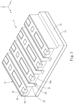
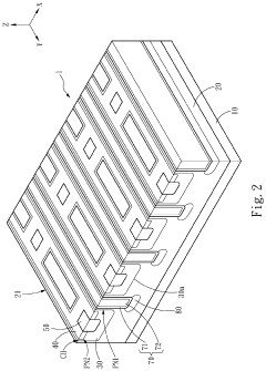
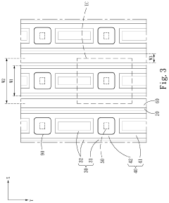
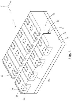
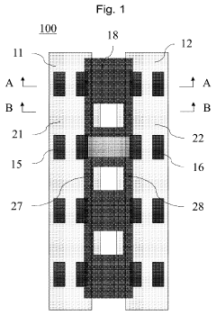
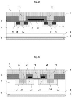
- A silicon carbide semiconductor device with a hybrid gate structure featuring a trench gate configuration that reduces JFET resistance and parasitic gate-to-drain capacitance, enhancing switching performance by increasing channel width density and optimizing the layout of doped regions and trenches.
Silicon carbide metal oxide semiconductor field effect transistor and manufacturing method of silicon carbide metal oxide semiconductor field effect transistor
PatentPendingUS20230378341A1
Innovation
- The design incorporates alternating cells with specific well regions, source regions, and contact layers, including ohmic and Schottky contacts, to reduce channel density, enhance short-circuit tolerance, and minimize reverse leakage current and forward voltage drop, while maintaining the transistor's size and functionality.
Supply Chain Considerations for SiC Materials
The SiC MOSFET supply chain presents unique challenges that significantly impact mass production capabilities. The raw material sourcing begins with high-purity silicon carbide substrates, which remain in limited supply globally. Currently, only a handful of suppliers such as Wolfspeed, II-VI Incorporated, and ROHM can produce wafers meeting the stringent quality requirements for power electronics applications. This supply concentration creates bottlenecks and potential vulnerabilities in the production ecosystem.
Material processing represents another critical consideration, as SiC is notoriously difficult to work with due to its extreme hardness (9.5 on the Mohs scale). The specialized equipment required for wafer processing, including high-temperature furnaces capable of exceeding 2000°C and precision cutting tools with diamond-tipped components, demands significant capital investment and specialized expertise that few manufacturers possess.
Geographic distribution of the supply chain introduces additional complexities. North America and Japan currently lead in substrate production, while China is rapidly expanding its capabilities through substantial government investments. This geographic dispersion necessitates complex logistics networks and increases vulnerability to regional disruptions, as evidenced during recent global supply chain crises.
Quality consistency across the supply chain remains problematic. The presence of micropipes, dislocations, and other crystalline defects in SiC wafers can dramatically reduce device yield and reliability. Establishing standardized quality metrics and testing protocols throughout the supply chain is essential but not yet fully realized across the industry.
Vertical integration strategies are increasingly being adopted by major players to mitigate supply risks. Companies like Infineon and STMicroelectronics have secured long-term supply agreements or acquired substrate manufacturers to ensure material availability. This trend toward consolidation may further concentrate market power among a few integrated manufacturers.
Cost structures throughout the supply chain significantly impact the economic viability of mass production. While SiC material costs have decreased by approximately 40% over the past decade, they remain 5-10 times higher than silicon alternatives. Economies of scale have not yet fully materialized due to relatively low production volumes compared to silicon technologies.
Sustainability considerations are gaining importance in supply chain management. The energy-intensive nature of SiC production raises environmental concerns, prompting research into more efficient manufacturing processes and recycling technologies to recover valuable materials from production waste and end-of-life devices.
Cost-Performance Trade-offs in SiC Manufacturing
The manufacturing of Silicon Carbide (SiC) MOSFETs presents significant cost-performance trade-offs that manufacturers must navigate carefully. Production costs for SiC devices remain substantially higher than traditional silicon counterparts, with raw wafer costs approximately 5-10 times higher. This cost differential stems from the complex crystal growth processes required for SiC, which involve higher temperatures and more sophisticated equipment than silicon manufacturing.
Material quality versus yield rate represents a critical trade-off. Higher-quality SiC substrates with fewer defects command premium prices but deliver better device performance and reliability. Manufacturers must determine whether investing in superior materials justifies the increased production costs, especially when considering the impact on final device pricing and market competitiveness.
Process complexity introduces another dimension to the cost-performance equation. The high-temperature annealing processes necessary for SiC device fabrication require specialized equipment and consume significant energy, driving up manufacturing expenses. However, these processes are essential for achieving the superior electrical characteristics that make SiC devices valuable in high-power applications.
Scale economies remain elusive in SiC manufacturing compared to silicon. While silicon benefits from decades of manufacturing optimization and massive production volumes, SiC fabrication has not yet achieved comparable economies of scale. This disparity means that performance improvements in SiC devices often come with disproportionate cost increases, creating challenging decisions for manufacturers regarding which performance parameters to prioritize.
Device design complexity further complicates the cost-performance balance. More sophisticated device architectures can deliver superior switching performance and lower on-resistance but require additional processing steps and more precise manufacturing controls. Manufacturers must evaluate whether the performance gains justify the increased production complexity and associated costs.
Market positioning considerations also influence these trade-offs. Premium SiC devices targeting specialized applications like electric vehicles or renewable energy systems can command higher prices, potentially justifying more expensive manufacturing approaches. Conversely, SiC devices aimed at price-sensitive markets may require manufacturing compromises to achieve competitive price points, even at the expense of optimal performance characteristics.
As the industry matures, manufacturers are developing innovative approaches to optimize these trade-offs, including selective performance targeting, process simplification, and vertical integration strategies. These efforts aim to deliver the most valuable performance characteristics while minimizing unnecessary manufacturing costs.
Unlock deeper insights with Patsnap Eureka Quick Research — get a full tech report to explore trends and direct your research. Try now!
Generate Your Research Report Instantly with AI Agent
Supercharge your innovation with Patsnap Eureka AI Agent Platform!
