

What Are The Common Application Mistakes With SiC MOSFETs?
SEP 8, 20259 MIN READ
Generate Your Research Report Instantly with AI Agent
PatSnap Eureka helps you evaluate technical feasibility & market potential.
SiC MOSFET Technology Background and Objectives
Silicon Carbide (SiC) MOSFETs represent a revolutionary advancement in power semiconductor technology, emerging as a superior alternative to traditional silicon-based devices in high-power applications. The evolution of SiC technology began in the early 1990s, with significant commercial breakthroughs occurring in the 2010s as manufacturing processes matured and costs decreased. This wide-bandgap semiconductor material offers fundamental advantages including higher breakdown electric field strength, superior thermal conductivity, and faster switching capabilities compared to silicon counterparts.
The technological trajectory of SiC MOSFETs has been characterized by continuous improvements in device performance, reliability, and cost-effectiveness. Early generations faced challenges with gate oxide reliability and high channel resistance, but recent advancements have substantially addressed these limitations. The current technological trend is moving toward higher voltage ratings (1700V and beyond), increased current densities, and enhanced ruggedness under extreme operating conditions.
Market adoption has accelerated dramatically in the past five years, driven primarily by electric vehicle traction inverters, renewable energy systems, and industrial power supplies. This adoption curve is expected to steepen as manufacturing scales and costs continue to decline. The technology has reached a critical inflection point where performance benefits increasingly outweigh cost premiums in many applications.
A primary objective in SiC MOSFET development is addressing common application mistakes that limit device performance and reliability. These include improper gate drive design, inadequate thermal management, suboptimal layout considerations, and insufficient protection against parasitic effects. Understanding and mitigating these application challenges is crucial for maximizing the benefits of SiC technology.
The technical goals for next-generation SiC MOSFETs include reducing on-resistance per unit area, improving short-circuit withstand capability, enhancing gate oxide reliability, and developing more sophisticated packaging solutions to handle higher power densities and switching frequencies. Additionally, there is significant focus on standardizing application methodologies to prevent common implementation errors.
Industry projections indicate that SiC MOSFETs will continue to penetrate medium and high-voltage applications, potentially capturing over 30% of the power semiconductor market in these segments by 2030. The technology is expected to enable new power conversion architectures that were previously impractical with silicon devices, particularly in applications requiring high efficiency, high temperature operation, or compact size.
Understanding the historical context, current capabilities, and future trajectory of SiC MOSFET technology provides essential foundation for addressing application challenges and developing best practices for implementation in power electronic systems.
Market Demand Analysis for SiC Power Devices
The Silicon Carbide (SiC) power device market has experienced remarkable growth in recent years, driven primarily by the increasing demand for high-efficiency power electronics across multiple industries. Market research indicates that the global SiC power device market is projected to grow at a CAGR of 29% from 2021 to 2026, reaching a market value of $2.5 billion by 2026.
The automotive sector represents the largest and fastest-growing application segment for SiC power devices. With the rapid expansion of electric vehicles (EVs), demand for SiC MOSFETs has surged due to their ability to significantly improve power conversion efficiency, reduce system size, and enhance thermal performance in EV powertrains and charging infrastructure. Major automotive manufacturers are increasingly adopting SiC technology in their newest EV models to extend driving range and reduce charging times.
Industrial applications constitute the second-largest market segment, with particular growth in motor drives, power supplies, and renewable energy systems. The superior switching characteristics of SiC MOSFETs enable higher frequency operation, resulting in smaller passive components and overall system size reduction. This has created strong demand in factory automation, HVAC systems, and industrial power supplies where space constraints and efficiency are critical factors.
In the renewable energy sector, SiC devices are gaining significant traction in solar inverters and wind power systems. The higher efficiency of SiC-based inverters translates directly to increased energy harvest from renewable sources, providing compelling economic benefits despite the higher initial component cost. Market analysis shows that SiC adoption in solar inverters is growing at 35% annually as manufacturers seek to differentiate their products through higher efficiency ratings.
The telecommunications and data center markets are emerging as important growth areas for SiC power devices. The push for energy efficiency in server power supplies and 5G infrastructure has created new opportunities for SiC MOSFETs in these applications. Power density requirements in these sectors align perfectly with SiC's performance advantages.
Regional analysis reveals that Asia-Pacific currently dominates the SiC power device market, accounting for approximately 45% of global demand. This is primarily due to the strong presence of automotive and industrial manufacturing in countries like China, Japan, and South Korea. North America and Europe follow closely, with particularly strong growth in EV-related applications.
Despite the compelling benefits, market penetration faces challenges related to cost premiums over traditional silicon devices and application knowledge gaps. Many potential users struggle with proper implementation of SiC MOSFETs, leading to reliability issues that slow adoption. Educational initiatives by major SiC manufacturers are helping to address these barriers and accelerate market growth.
Current Challenges in SiC MOSFET Implementation
Despite the promising advantages of Silicon Carbide (SiC) MOSFETs, their implementation faces several significant challenges that hinder widespread adoption. One primary obstacle is the higher cost compared to traditional silicon-based devices, with SiC MOSFETs typically commanding a 2-3x price premium. This cost differential creates a substantial barrier, particularly for price-sensitive applications where the performance benefits may not immediately justify the increased expense.
The reliability and robustness of SiC MOSFETs under various operating conditions remain concerns for many system designers. These devices exhibit different failure modes compared to silicon MOSFETs, including increased sensitivity to short-circuit events and potential degradation of gate oxide over time. The limited field data on long-term reliability creates uncertainty for applications requiring extended operational lifetimes.
Design engineers face significant challenges in optimizing gate drive circuits for SiC MOSFETs. The devices require more precise gate voltage control (typically +15V/-5V) compared to silicon counterparts, with narrower tolerance bands. Additionally, the faster switching speeds of SiC MOSFETs (often 5-10 times faster than silicon) necessitate careful consideration of layout parasitic elements to prevent ringing, overshoot, and potential device failure.
Thermal management presents another substantial challenge. While SiC devices can operate at higher temperatures (up to 175-200°C junction temperature), this capability often requires specialized packaging solutions and thermal interface materials. The higher power density also creates concentrated heat zones that demand innovative cooling strategies beyond traditional approaches used with silicon devices.
EMI/EMC compliance has emerged as a critical challenge due to the extremely fast switching transients of SiC MOSFETs. The high dv/dt and di/dt rates can generate significant electromagnetic interference, requiring additional filtering components and careful system layout. This often negates some of the size and efficiency advantages initially promised by SiC technology.
System integration challenges extend to protection circuits, which must respond much faster to fault conditions due to the reduced short-circuit withstand time of SiC devices (typically 1-2 μs compared to 10+ μs for silicon). This necessitates redesigned protection schemes with response times in the sub-microsecond range.
Finally, there exists a significant knowledge gap in the engineering community regarding SiC MOSFET implementation best practices. Many design engineers have decades of experience with silicon devices but limited exposure to wide bandgap technologies, leading to suboptimal designs that fail to fully leverage SiC capabilities or, worse, result in premature device failures.
Common Application Mistakes and Best Practices
01 SiC MOSFET structure and fabrication
Silicon Carbide (SiC) MOSFETs have unique structural features and fabrication methods that enhance their performance characteristics. These include specialized gate structures, channel designs, and manufacturing techniques that improve electron mobility and reduce on-resistance. The fabrication processes often involve specific thermal treatments, ion implantation techniques, and epitaxial growth methods tailored for SiC material properties to achieve optimal device performance.- SiC MOSFET structure and fabrication: Silicon Carbide (SiC) MOSFETs have unique structural features and fabrication methods that enhance their performance characteristics. These include specialized gate structures, channel designs, and manufacturing techniques that improve electron mobility and reduce on-resistance. The fabrication processes often involve specific thermal oxidation steps, ion implantation methods, and annealing procedures that are optimized for the SiC material system to achieve high-quality gate oxide interfaces and reliable device operation.
- Power conversion applications of SiC MOSFETs: SiC MOSFETs are widely used in power conversion systems due to their superior switching characteristics and high-temperature operation capabilities. These devices enable more efficient power conversion in applications such as inverters, converters, and motor drives. The implementation of SiC MOSFETs in these systems results in reduced switching losses, higher operating frequencies, and improved thermal management, leading to overall system size reduction and increased power density.
- Gate driver designs for SiC MOSFETs: Specialized gate driver circuits are essential for optimal operation of SiC MOSFETs. These drivers are designed to handle the unique switching characteristics and gate voltage requirements of SiC devices. Advanced gate driver designs incorporate features such as adjustable slew rate control, protection against voltage spikes, and temperature compensation mechanisms. These circuits ensure reliable switching performance while minimizing losses and protecting the device from operational stresses.
- Thermal management and reliability of SiC MOSFETs: Effective thermal management is crucial for SiC MOSFETs to maintain reliability and performance under high-power operation. Various packaging technologies and cooling solutions are employed to dissipate heat efficiently from these devices. Reliability enhancement techniques include specialized die-attach materials, optimized wire bonding methods, and conformal coatings that protect against environmental factors. These approaches extend device lifetime and maintain stable electrical characteristics under extreme operating conditions.
- Testing and characterization methods for SiC MOSFETs: Specialized testing and characterization methods are developed for evaluating SiC MOSFET performance and reliability. These include techniques for measuring switching characteristics, on-resistance, threshold voltage stability, and breakdown behavior. Advanced testing protocols incorporate accelerated stress testing, temperature cycling, and gate oxide reliability assessment. These methods help in qualifying devices for demanding applications and provide data for continuous improvement of device designs and manufacturing processes.
02 Power conversion applications of SiC MOSFETs
SiC MOSFETs are widely used in power conversion systems due to their superior switching characteristics and high voltage handling capabilities. These devices enable more efficient power conversion in applications such as inverters, converters, and power supplies. Their fast switching speeds, low switching losses, and high temperature operation capabilities make them ideal for high-frequency power conversion circuits, resulting in smaller, more efficient power systems.Expand Specific Solutions03 SiC MOSFET driving circuits and gate control
Specialized driving circuits and gate control methods are essential for optimizing SiC MOSFET performance. These include advanced gate driver designs that address the unique switching characteristics of SiC devices, protection circuits to prevent overvoltage and overcurrent conditions, and control strategies that minimize switching losses. Proper gate voltage control and timing are critical for achieving the full benefits of SiC technology while ensuring reliable operation.Expand Specific Solutions04 Thermal management and reliability of SiC MOSFETs
Effective thermal management is crucial for SiC MOSFETs to maintain reliability and performance. This includes innovative packaging designs, heat dissipation structures, and thermal interface materials that can handle the high power density of these devices. Reliability enhancement techniques address specific failure mechanisms in SiC devices, such as gate oxide integrity, threshold voltage stability, and body diode performance under various operating conditions.Expand Specific Solutions05 SiC MOSFET integration in circuit design
Integration of SiC MOSFETs into circuit designs requires specific considerations to leverage their unique characteristics. This includes optimized PCB layouts that minimize parasitic inductances, specialized protection schemes, and circuit topologies that take advantage of the high-frequency operation capabilities. System-level design approaches incorporate SiC MOSFETs to achieve higher power density, improved efficiency, and reduced system size in applications ranging from automotive powertrains to renewable energy systems.Expand Specific Solutions
Key Manufacturers and Competitors in SiC MOSFET Market
The SiC MOSFET application landscape is currently in a growth phase, with the market expected to reach $2.5 billion by 2025 as industries transition from silicon to wide bandgap semiconductors. Key players like ROHM, Infineon, and GeneSiC are leading technological innovation, while emerging competitors from China including Yangjie Electronic and Beijing Century Goldray are rapidly advancing their capabilities. The technology has reached moderate maturity in power conversion applications but still faces implementation challenges related to gate driving, thermal management, and switching behavior. Research collaborations between industry leaders and academic institutions such as Nanjing University and Chongqing University are accelerating development of application-specific solutions to address common mistakes in SiC MOSFET implementation.
ROHM Co., Ltd.
Technical Solution: ROHM has pioneered solutions for common SiC MOSFET application mistakes through their SCT technology platform. Their approach includes specialized gate driver ICs (such as the BM61S40RFV-C) specifically designed for SiC MOSFETs with optimized driving parameters to prevent gate oxide stress and threshold voltage instability. ROHM's technology incorporates a unique short-circuit withstand capability enhancement that provides extended protection time (>2μs) compared to conventional devices. Their SiC MOSFETs feature proprietary trench gate structures that reduce on-resistance while maintaining high short-circuit ruggedness. ROHM has also developed specialized thermal simulation tools and application guidelines that help engineers avoid common thermal management mistakes, including detailed junction temperature calculations and cooling system recommendations tailored specifically for SiC's unique thermal characteristics.
Strengths: Vertically integrated manufacturing from SiC wafer to module level, ensuring quality control; specialized gate driver solutions optimized for their SiC devices; extensive application support resources. Weaknesses: More limited voltage range offerings compared to some competitors; higher cost premium for their fully integrated solutions; requires careful attention to layout recommendations.
Mitsubishi Electric Corp.
Technical Solution: Mitsubishi Electric addresses common SiC MOSFET application mistakes through their DIPIPM™-SiC power module technology. Their approach integrates optimized gate drive circuitry directly within power modules, eliminating many common external gate drive design errors. Mitsubishi's technology features proprietary chip technology with enhanced short-circuit withstand capability (>2μs) and optimized internal gate resistance to control switching transients. Their modules incorporate advanced thermal management solutions with direct liquid cooling options that address the higher power density challenges of SiC implementations. Mitsubishi has developed comprehensive application guidelines specifically addressing parasitic inductance minimization in module designs, with their latest generations achieving below 10nH stray inductance. Additionally, they provide specialized protection schemes for SiC devices that account for their different short-circuit behavior compared to silicon IGBTs.
Strengths: Highly integrated power module solutions that eliminate many common design mistakes; extensive experience in high power applications; advanced thermal management solutions. Weaknesses: Higher cost premium for integrated solutions; more focused on higher power applications with fewer options for lower power designs; requires specialized cooling systems for optimal performance.
Critical Technical Analysis of SiC MOSFET Design Issues
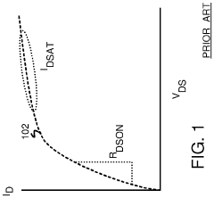
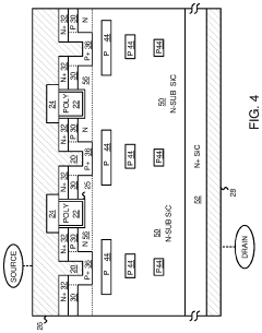
Sic mosfet with transverse p+ region
PatentActiveUS20230053874A1
Innovation
- The design incorporates a silicon carbide MOSFET structure with specific doping layers and geometries, including a polysilicon gate layer, to enhance the protection of the gate oxide without increasing the MOSFET cell area, utilizing epitaxy and ion implantation processes to create N+ and P+ regions that act as shields, ensuring adequate body diode performance and channel mobility.
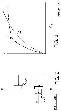
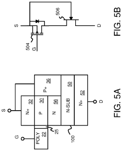
Silicon-Carbide (SiC) Metal-Oxide-Semiconductor Field-Effect Transistor (MOSFET) with Short Circuit Protection
PatentActiveUS20230327018A1
Innovation
- An integrated MOSFET-JFET device with ON-resistance trimming p-islands is developed, where the geometry of p-islands shapes the I-V curve to reduce ON resistance in the linear region and saturation current, providing better short-circuit protection and efficiency.
Thermal Management Considerations for SiC MOSFETs
Thermal management is a critical aspect of SiC MOSFET implementation that is frequently misunderstood or improperly addressed in applications. The superior thermal conductivity of silicon carbide (approximately 3 times that of silicon) creates a false sense of security among engineers who may underestimate the thermal challenges these devices present. Despite their enhanced thermal properties, SiC MOSFETs generate significant heat during operation due to their capability to handle higher power densities and switching frequencies.
One common mistake is the improper design of cooling systems based on silicon MOSFET thermal models. SiC devices operate at much higher junction temperatures (typically up to 175°C compared to 150°C for silicon), requiring recalibration of thermal design parameters. Engineers often fail to account for this extended temperature range, leading to premature thermal throttling or device failure.
The thermal interface material (TIM) selection represents another critical oversight. The higher power density of SiC MOSFETs demands TIMs with superior thermal conductivity and long-term reliability at elevated temperatures. Standard TIMs designed for silicon applications may degrade rapidly under SiC operating conditions, creating thermal bottlenecks that compromise system performance.
PCB layout considerations are frequently neglected in thermal management strategies. The concentrated heat generation in SiC devices requires careful attention to copper thickness, thermal vias placement, and component spacing. Inadequate copper pour or insufficient thermal vias can create hotspots that accelerate device aging and reduce reliability, even when the overall junction temperature appears within specifications.
Dynamic thermal management presents unique challenges with SiC MOSFETs. Their faster switching capabilities mean thermal transients occur more rapidly than in silicon devices. Conventional temperature sensing methods may lack the response time to detect these rapid thermal excursions, potentially allowing dangerous temperature spikes to go undetected.
The interaction between electrical and thermal performance is often overlooked. As temperature increases, SiC MOSFETs experience changes in on-resistance and switching characteristics that can further increase losses, creating a positive feedback loop of thermal runaway if not properly managed. Engineers must implement comprehensive thermal monitoring and protection schemes that account for these complex interactions.
Advanced cooling technologies such as direct liquid cooling, phase-change materials, or advanced heat pipe designs may be necessary for high-performance SiC applications but are frequently omitted in favor of traditional heatsink solutions that prove inadequate under sustained high-power operation.
Reliability and Lifetime Assessment of SiC Power Devices
The reliability and lifetime assessment of Silicon Carbide (SiC) MOSFETs represents a critical area of study as these devices continue to gain prominence in power electronics applications. Unlike traditional silicon-based devices, SiC MOSFETs exhibit unique degradation mechanisms that must be thoroughly understood to ensure long-term operational stability.
Accelerated lifetime testing methodologies have been developed specifically for SiC power devices, including High Temperature Gate Bias (HTGB) and High Temperature Reverse Bias (HTRB) tests. These tests subject devices to extreme conditions to induce accelerated aging, providing valuable data on potential failure modes. Time-Dependent Dielectric Breakdown (TDDB) testing has emerged as particularly relevant for SiC MOSFETs due to their thinner gate oxide layers compared to silicon counterparts.
Field reliability data indicates that threshold voltage instability remains one of the primary concerns affecting SiC MOSFET longevity. This instability manifests as a shift in threshold voltage over time, potentially leading to unpredictable switching behavior. Research has shown that this phenomenon is exacerbated by common application mistakes, including improper gate drive design and voltage overshoots during switching transitions.
Body diode reliability presents another significant challenge. Unlike silicon devices, SiC MOSFETs experience stacking fault formation during body diode conduction, which can lead to increased on-resistance over time. This degradation mechanism is often overlooked in application designs, resulting in premature device failure when the body diode is utilized extensively.
Statistical lifetime prediction models have been developed to quantify the impact of these degradation mechanisms. The Weibull distribution has proven particularly effective for modeling SiC MOSFET failure rates, with shape parameters typically ranging from 2.3 to 3.1 depending on the specific failure mode. These models enable more accurate Mean Time To Failure (MTTF) predictions when properly calibrated with experimental data.
Temperature cycling and power cycling tests reveal that package-related failures often precede die-related failures in SiC MOSFETs. The coefficient of thermal expansion mismatch between SiC and packaging materials creates mechanical stress that can lead to bond wire lift-off or solder fatigue. Advanced packaging technologies, including silver sintering and copper clip bonding, have demonstrated improved reliability metrics compared to traditional aluminum wire bonding approaches.
Recent advancements in online condition monitoring techniques allow for real-time assessment of SiC MOSFET health status. Parameters such as on-resistance, threshold voltage, and junction temperature can be continuously monitored to predict impending failures before they occur, enabling preventive maintenance strategies in critical applications.
Unlock deeper insights with PatSnap Eureka Quick Research — get a full tech report to explore trends and direct your research. Try now!
Generate Your Research Report Instantly with AI Agent
Supercharge your innovation with PatSnap Eureka AI Agent Platform!