Comparative Analysis of Silicon Carbide Wafer vs Traditional Silicon
OCT 14, 20259 MIN READ
Generate Your Research Report Instantly with AI Agent
Patsnap Eureka helps you evaluate technical feasibility & market potential.
SiC vs Si Wafer Technology Background and Objectives
Silicon carbide (SiC) wafer technology represents a significant evolution in semiconductor materials, emerging as a compelling alternative to traditional silicon (Si) wafers that have dominated the industry for decades. The development of SiC technology can be traced back to the early 1900s when it was first synthesized, though commercial viability for semiconductor applications only materialized in recent decades. The technological trajectory has accelerated notably since the 2010s, with substantial improvements in crystal growth techniques, defect reduction, and wafer size expansion.
The fundamental advantage of SiC lies in its superior material properties. With a bandgap approximately three times wider than silicon (3.2 eV versus 1.1 eV), SiC demonstrates remarkable thermal conductivity (3-4 times higher than Si) and breakdown electric field strength (10 times greater than Si). These intrinsic characteristics enable SiC-based devices to operate at significantly higher temperatures, voltages, and frequencies while maintaining reliability.
The evolution of SiC wafer technology has progressed through several critical phases, beginning with small-diameter, defect-prone substrates to today's commercially available 6-inch wafers with dramatically improved quality. Industry roadmaps indicate imminent expansion to 8-inch wafers, gradually approaching the economies of scale enjoyed by silicon's established 12-inch standard. This progression reflects the industry's commitment to overcoming SiC's historical limitations.
The primary technical objectives driving SiC development include achieving cost parity with silicon through improved manufacturing yields and economies of scale. Current SiC wafers remain 5-10 times more expensive than their silicon counterparts, presenting a significant barrier to widespread adoption. Additional objectives focus on reducing crystal defects such as micropipes, dislocations, and basal plane defects that compromise device performance and reliability.
From a market perspective, SiC technology aims to establish dominance in high-power, high-temperature, and high-frequency applications where silicon reaches fundamental physical limitations. The electric vehicle sector represents a particularly promising target, with SiC power electronics enabling more efficient power conversion, faster charging capabilities, and extended range through reduced energy losses.
Looking forward, the technological trajectory suggests continued refinement of crystal growth processes, particularly through advancements in physical vapor transport (PVT) and modified Lely methods. Parallel development efforts focus on epitaxial growth optimization, novel device architectures, and packaging solutions specifically designed to leverage SiC's unique thermal and electrical properties. These combined advances aim to position SiC as the material of choice for next-generation power electronics, potentially disrupting silicon's long-standing dominance in specific high-performance application segments.
Market Demand Analysis for Wide Bandgap Semiconductors
The wide bandgap (WBG) semiconductor market has experienced significant growth in recent years, driven primarily by the superior performance characteristics these materials offer compared to traditional silicon. Silicon carbide (SiC), as a leading WBG material, has seen particularly strong demand growth across multiple sectors. The global SiC market was valued at approximately $2.52 billion in 2022 and is projected to reach $7.18 billion by 2030, representing a compound annual growth rate of nearly 14%.
Power electronics applications constitute the largest segment of the WBG semiconductor market, accounting for over 60% of total demand. This is largely attributable to the increasing adoption of electric vehicles (EVs), where SiC-based power modules offer substantial efficiency improvements over traditional silicon. Major automotive manufacturers have begun integrating SiC power electronics into their EV designs, with some reporting range improvements of 5-10% compared to silicon-based alternatives.
The renewable energy sector represents another significant market for WBG semiconductors, particularly SiC. Solar inverters and wind power systems benefit from the higher switching frequencies and reduced power losses that SiC devices provide. Market research indicates that SiC-based inverters can achieve efficiency ratings exceeding 99%, compared to 96-97% for traditional silicon solutions, translating to meaningful energy savings at utility scale.
Industrial applications form the third major demand driver, with factory automation, motor drives, and uninterruptible power supplies increasingly adopting SiC technology. The industrial sector values the reduced cooling requirements and smaller form factors enabled by SiC's superior thermal conductivity and breakdown field strength.
Regional analysis reveals that Asia-Pacific currently dominates the WBG semiconductor market with approximately 45% share, followed by North America at 30% and Europe at 20%. China has made significant investments in developing domestic SiC manufacturing capabilities, recognizing the strategic importance of this technology for its industrial and automotive sectors.
Market forecasts indicate that the demand-supply gap for SiC wafers will persist through at least 2025, with wafer manufacturers operating at near-capacity levels despite ongoing expansion efforts. This supply constraint has maintained upward pressure on SiC wafer prices, which remain 5-10 times higher than comparable silicon wafers depending on diameter and quality specifications.
Consumer awareness of energy efficiency and sustainability considerations is further accelerating market adoption of WBG semiconductors. Government regulations targeting carbon emissions reduction and energy conservation across multiple industries have created additional tailwinds for SiC adoption, with several countries implementing incentive programs specifically for technologies that enable electrification and improved power conversion efficiency.
Current State and Challenges in SiC Wafer Production
Silicon Carbide (SiC) wafer production currently faces significant technical and economic challenges despite its promising advantages over traditional silicon. Global production capacity remains limited, with only a handful of manufacturers capable of producing high-quality SiC wafers at commercial scale. The primary production method involves physical vapor transport (PVT), which requires extremely high temperatures (over 2000°C) and precise control of growth conditions, making it substantially more complex than silicon wafer production.
The most pressing technical challenge is defect density reduction. SiC wafers typically contain various crystallographic defects including micropipes, dislocations, stacking faults, and basal plane dislocations that significantly impact device performance. While micropipe densities have been reduced to near-zero levels in recent years, other defect types continue to limit yield and performance. Current state-of-the-art 6-inch SiC wafers still exhibit defect densities approximately 10-100 times higher than those in mature silicon technology.
Wafer size scaling represents another major hurdle. While silicon technology has advanced to 300mm (12-inch) wafers, SiC production remains predominantly at 150mm (6-inch), with 200mm (8-inch) wafers only beginning to emerge in commercial settings. This size limitation directly impacts economies of scale and integration with existing semiconductor manufacturing infrastructure, which is increasingly optimized for larger wafer sizes.
Material quality consistency poses additional challenges. Variations in dopant concentration, polytype inclusions (unwanted 3C-SiC in 4H-SiC wafers), and surface roughness affect device performance and manufacturing yield. The industry still struggles to achieve the tight specifications and uniformity standards that silicon wafer production has mastered over decades.
Cost remains perhaps the most significant barrier to widespread adoption. Current SiC wafers are approximately 5-10 times more expensive than silicon wafers of comparable size, primarily due to complex manufacturing processes, lower yields, smaller wafer sizes, and limited production volumes. This cost differential makes SiC economically viable only for high-value applications where its performance advantages clearly justify the premium.
Geographically, SiC wafer production is concentrated in a few regions, with the United States, Japan, and Europe leading development. China has made significant investments to build domestic capacity but still lags in producing the highest quality wafers. This concentration creates potential supply chain vulnerabilities as demand increases with wider adoption of electric vehicles and renewable energy systems.
Recent advancements in epitaxial growth techniques and defect characterization methods have improved production capabilities, but significant R&D investment is still required to overcome these challenges and achieve cost parity with silicon for broader market penetration.
Current Technical Solutions for SiC Wafer Fabrication
01 Material properties comparison between SiC and Si wafers
Silicon carbide (SiC) wafers offer superior material properties compared to traditional silicon wafers, including higher thermal conductivity, greater bandgap, and higher breakdown electric field strength. These properties make SiC particularly suitable for high-power, high-temperature, and high-frequency applications where traditional silicon has limitations. The crystalline structure of SiC provides better mechanical strength and chemical resistance, allowing devices to operate in harsh environments.- Material Properties and Advantages of SiC vs Si Wafers: Silicon carbide (SiC) wafers offer superior material properties compared to traditional silicon wafers, including wider bandgap, higher thermal conductivity, and greater breakdown electric field strength. These properties make SiC particularly advantageous for high-power, high-temperature, and high-frequency applications where traditional silicon has limitations. The enhanced thermal stability of SiC allows devices to operate at temperatures exceeding 600°C, while silicon-based devices typically cannot exceed 150°C without performance degradation.
- Manufacturing Processes for SiC Wafers: The manufacturing of silicon carbide wafers involves specialized processes that differ significantly from traditional silicon wafer production. These include sublimation growth methods, chemical vapor deposition (CVD), and physical vapor transport (PVT) for crystal growth. SiC wafer production requires higher temperatures (typically above 2000°C) and more complex processing steps to achieve high-quality crystals with minimal defects. The manufacturing challenges include reducing micropipe defects, controlling polytype formation, and achieving larger diameter wafers comparable to silicon.
- Device Applications and Performance Comparison: Silicon carbide wafers enable the development of high-performance semiconductor devices that outperform traditional silicon-based counterparts in specific applications. SiC-based power devices such as MOSFETs, Schottky diodes, and JFETs demonstrate lower switching losses, higher blocking voltages, and better efficiency in power conversion systems. These advantages make SiC particularly valuable in electric vehicles, renewable energy systems, industrial motor drives, and high-voltage transmission equipment where energy efficiency and thermal management are critical considerations.
- Integration Challenges and Hybrid Solutions: Integrating silicon carbide technology with existing silicon-based infrastructure presents significant challenges that require innovative solutions. These challenges include interface issues between SiC and other materials, specialized packaging requirements, and compatibility with established fabrication processes. Hybrid approaches combining SiC and Si technologies on the same system allow manufacturers to leverage the advantages of both materials. Various techniques have been developed to address these integration challenges, including specialized bonding methods, buffer layers, and heterogeneous integration platforms.
- Economic Considerations and Market Adoption: Despite the superior performance of silicon carbide wafers, economic factors significantly influence their market adoption compared to traditional silicon. SiC wafers typically cost 5-10 times more than silicon wafers of comparable size, primarily due to complex manufacturing processes and lower production volumes. The semiconductor industry is gradually increasing SiC wafer adoption as manufacturing techniques improve and costs decrease. Market trends show growing demand for SiC in automotive, industrial, and power electronics sectors where the performance benefits justify the higher costs, while silicon remains dominant in consumer electronics and applications where cost sensitivity outweighs performance requirements.
02 Manufacturing processes for SiC wafers
Manufacturing silicon carbide wafers involves specialized processes that differ from traditional silicon wafer production. These include sublimation growth methods, chemical vapor deposition (CVD), and advanced cutting and polishing techniques to handle the harder SiC material. The production process requires higher temperatures and pressures compared to silicon wafer manufacturing, resulting in higher production costs but yielding wafers with superior properties for specific applications.Expand Specific Solutions03 Device performance improvements with SiC
Devices fabricated on silicon carbide wafers demonstrate significant performance improvements over traditional silicon-based devices in specific applications. These include higher efficiency power electronics, reduced switching losses, better thermal management, and improved reliability at elevated temperatures. SiC-based devices can operate at junction temperatures exceeding 200°C, whereas silicon devices are typically limited to around 150°C. The wider bandgap of SiC also enables higher blocking voltages and faster switching speeds.Expand Specific Solutions04 Integration challenges and hybrid solutions
Integrating silicon carbide technology with existing silicon-based infrastructure presents several challenges, including interface compatibility issues, different thermal expansion coefficients, and specialized processing requirements. To address these challenges, hybrid solutions combining both materials have been developed, allowing gradual adoption of SiC technology while leveraging existing silicon manufacturing infrastructure. These approaches include SiC-on-Si substrates, heterogeneous integration techniques, and specialized bonding methods.Expand Specific Solutions05 Economic and scaling considerations
Despite the superior technical performance of silicon carbide wafers, economic factors and scaling challenges affect their widespread adoption compared to traditional silicon. SiC wafers typically cost 5-10 times more than silicon wafers of comparable size, and are generally available in smaller diameters (up to 6-8 inches compared to 12 inches for silicon). Manufacturing defect densities are also higher for SiC. However, ongoing research and development are focused on reducing these cost differentials and improving manufacturing yields to make SiC more competitive for broader applications.Expand Specific Solutions
Key Industry Players in SiC Wafer Manufacturing
Silicon Carbide (SiC) wafer technology is rapidly transforming the semiconductor landscape, currently in a growth phase with market expansion driven by power electronics and electric vehicle applications. The global SiC market is experiencing robust growth, projected to reach significant scale as industries transition from traditional silicon. Companies like Wolfspeed, STMicroelectronics, and Infineon Technologies lead in technological maturity, with established manufacturing capabilities and product portfolios. RESONAC, GlobalWafers, and TanKeBlue are emerging as significant suppliers, while automotive giants Toyota and DENSO are investing heavily in SiC applications. Research institutions like Shandong University and industrial players such as SICC are advancing manufacturing processes, indicating a competitive landscape where established semiconductor manufacturers compete with specialized SiC-focused companies across the value chain.
STMicroelectronics International NV
Technical Solution: STMicroelectronics has developed a comprehensive silicon carbide technology platform called STPOWER SiC. Their approach includes proprietary substrate preparation techniques and epitaxial growth processes that achieve doping uniformity variation below 5% across 150mm wafers. ST's manufacturing process incorporates specialized implantation and activation annealing at temperatures exceeding 1700°C to achieve optimal dopant activation in SiC, significantly higher than silicon's typical 1000-1100°C processes. Their SiC MOSFETs feature a unique double-implanted structure that reduces on-resistance by approximately 40% compared to conventional designs while maintaining breakdown voltages above 1200V. ST has also pioneered advanced edge termination structures that improve device reliability under high-temperature operation, enabling continuous operation at junction temperatures up to 200°C, compared to silicon's typical 150°C limit. Their recent advancements include specialized backside processing techniques that reduce wafer bow to less than 20μm, enabling compatibility with standard semiconductor equipment.
Strengths: Fully integrated manufacturing from substrate to packaged devices; advanced process technology with high yield rates; strong automotive qualification program. Weaknesses: Higher manufacturing costs compared to silicon technologies; challenges in scaling to 200mm wafers; limited substrate supplier diversity creating supply chain vulnerabilities.
Sumitomo Electric Industries Ltd.
Technical Solution: Sumitomo Electric has developed advanced silicon carbide wafer manufacturing technology focused on high-quality substrate production. Their proprietary Physical Vapor Transport (PVT) crystal growth method achieves growth rates exceeding 0.5mm/hour while maintaining low defect densities. Sumitomo's SiC wafers feature micropipe densities below 0.5cm² and basal plane dislocations below 1000cm², significantly better than industry averages. Their manufacturing process includes specialized high-temperature annealing techniques that reduce residual stress in SiC crystals, resulting in wafers with bow and warp measurements below 10μm for 150mm diameter wafers. Sumitomo has also developed unique surface preparation methods that achieve atomically flat surfaces with step heights of single silicon-carbon bilayers (0.25nm), enabling more uniform epitaxial growth. Their recent innovations include specialized slicing techniques that improve material utilization by over 30% compared to conventional methods, reducing the overall cost of SiC wafer production.
Strengths: Industry-leading substrate quality with extremely low defect densities; advanced crystal growth technology enabling larger diameter wafers; strong vertical integration with epitaxial growth capabilities. Weaknesses: Limited production capacity compared to silicon; higher manufacturing costs; challenges in scaling to 200mm diameter wafers while maintaining quality standards.
Critical Patents and Innovations in SiC Wafer Technology
Sic single crystal wafer and process for production thereof
PatentPendingEP2471981A1
Innovation
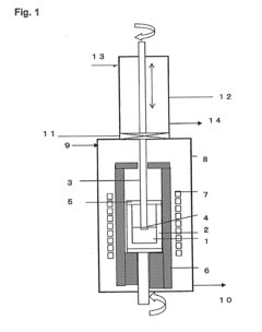
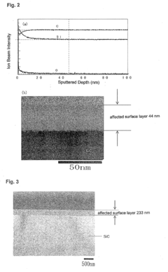
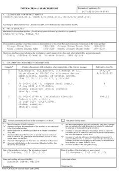
- The method involves controlling the oxygen concentration in the SiC single crystal portion to reduce the thickness of the affected surface layer to at most 50 nm, allowing for precise in situ etching and eliminating the subsurface damaged layer and native oxide film, thereby ensuring a smooth epitaxial growth surface.
Silicon carbide single-crystal wafer and process for producing the same
PatentInactiveEP1895573A1
Innovation
- A method involving cutting silicon carbide wafers at specific OFF angles (less than 2°) and OFF directions (less than 10° from the (11-20) direction, followed by surface processing and controlled chemical vapor deposition to grow epitaxial films with reduced defects and improved flatness, using a C/Si ratio of 1.5 or less and reacting gases at 1550 to 1700°C.
Environmental Impact and Sustainability Considerations
The environmental footprint of semiconductor manufacturing represents a critical consideration in the industry's sustainable development. Silicon Carbide (SiC) wafers demonstrate significant environmental advantages over traditional silicon wafers throughout their lifecycle. The manufacturing process for SiC wafers, while energy-intensive, ultimately results in devices that operate at higher temperatures and voltages with substantially reduced energy losses compared to silicon-based alternatives.
Energy efficiency gains from SiC implementation are particularly notable in power electronics applications. Studies indicate that SiC-based power devices can reduce energy consumption by 15-35% in electric vehicles, renewable energy systems, and industrial motor drives. This translates to meaningful carbon emission reductions when assessed from a complete product lifecycle perspective.
Water usage presents another important environmental metric. Traditional silicon wafer production requires approximately 8-10 gallons of ultra-pure water per square inch of wafer. SiC manufacturing processes have demonstrated potential for 20-30% reduction in water consumption through optimized cleaning cycles and improved recycling systems, though implementation varies significantly between manufacturers.
Chemical utilization and waste generation also favor SiC technology. The higher durability of SiC wafers extends device lifespans, reducing electronic waste generation. Additionally, SiC devices contain fewer toxic materials compared to certain specialized silicon wafer applications that require arsenic, phosphorus, or boron in higher concentrations.
Raw material sourcing represents a sustainability challenge for both technologies. Silicon is abundant, constituting approximately 28% of the Earth's crust. Silicon carbide requires carbon sources alongside silicon, typically derived from petroleum products. However, research into sustainable carbon sources, including biomass-derived alternatives, shows promise for reducing the environmental impact of SiC wafer production.
End-of-life considerations increasingly favor SiC technology. The chemical stability and higher value of SiC materials create stronger economic incentives for recycling compared to traditional silicon. Several manufacturers have established recycling programs specifically for SiC production waste and end-of-life devices, recovering valuable materials and reducing landfill impact.
Regulatory frameworks worldwide are evolving to prioritize energy-efficient technologies, with the European Union's Ecodesign Directive and similar initiatives in North America and Asia providing incentives for SiC adoption. These frameworks recognize the downstream environmental benefits that offset the initially higher manufacturing footprint of SiC wafers.
Cost-Benefit Analysis of SiC vs Si Implementation
The implementation of Silicon Carbide (SiC) technology versus traditional Silicon (Si) presents a complex cost-benefit equation that organizations must carefully evaluate. Initial capital expenditure for SiC-based systems is significantly higher, with SiC wafers costing approximately 3-5 times more than their silicon counterparts. This price differential stems from manufacturing complexities, lower production volumes, and higher defect rates in SiC wafer production processes.
Manufacturing infrastructure represents another substantial cost factor. Facilities equipped for Si production require considerable modifications or complete overhauls to accommodate SiC processing requirements, including higher temperature capabilities and specialized handling equipment. These transition costs can range from millions to billions depending on facility scale and production volume targets.
Despite these higher upfront investments, SiC implementations deliver compelling long-term operational benefits. Energy efficiency improvements of 20-40% compared to Si-based systems translate to substantial operational cost savings over product lifetimes. This efficiency advantage becomes particularly significant in high-power applications where energy consumption represents a major operational expense.
Maintenance requirements and system longevity further strengthen SiC's economic case. SiC-based systems demonstrate superior reliability with mean time between failures (MTBF) rates 2-3 times better than silicon equivalents. This reliability advantage reduces maintenance costs and extends operational lifespans, improving total cost of ownership calculations despite higher acquisition costs.
Market positioning benefits must also factor into the analysis. Products incorporating SiC technology command premium pricing due to performance advantages, potentially offsetting higher component costs. Additionally, early adoption of SiC technology can establish competitive differentiation and technological leadership in rapidly evolving markets like electric vehicles and renewable energy.
Regulatory considerations increasingly favor SiC adoption. As energy efficiency standards tighten globally, SiC solutions more readily meet or exceed these requirements, potentially avoiding compliance penalties or enabling access to incentive programs that improve the economic equation.
The cost-benefit analysis ultimately depends on application-specific factors including power requirements, operational duration, energy costs, and performance demands. While consumer electronics with short replacement cycles may struggle to justify SiC implementation, industrial systems, power infrastructure, and transportation applications with longer operational lifespans typically achieve positive return on investment despite higher initial costs.
Unlock deeper insights with Patsnap Eureka Quick Research — get a full tech report to explore trends and direct your research. Try now!
Generate Your Research Report Instantly with AI Agent
Supercharge your innovation with Patsnap Eureka AI Agent Platform!