Comparative Study of Silicon Carbide Wafer vs Gallium Nitride
OCT 14, 20259 MIN READ
Generate Your Research Report Instantly with AI Agent
Patsnap Eureka helps you evaluate technical feasibility & market potential.
SiC and GaN Semiconductor Evolution and Objectives
Silicon Carbide (SiC) and Gallium Nitride (GaN) represent the vanguard of wide bandgap semiconductor materials, marking a significant evolution beyond traditional silicon-based technologies. The development of SiC can be traced back to the early 1900s, with its first commercial applications emerging in the 1990s for power electronics. GaN's semiconductor journey began later, in the 1990s, initially revolutionizing the LED industry before expanding into power electronics in the early 2000s.
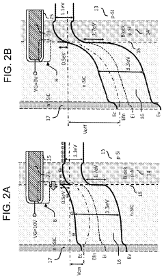
The evolution of these materials has been driven by increasing demands for higher efficiency, greater power density, and operation in extreme environments where silicon reaches its physical limitations. SiC offers a bandgap of approximately 3.3 eV compared to silicon's 1.1 eV, while GaN provides an even wider bandgap of 3.4 eV. These properties enable devices that can withstand higher voltages, operate at higher temperatures, and switch at higher frequencies with reduced losses.
Market adoption has followed distinct trajectories, with SiC gaining traction first in industrial applications and more recently in electric vehicles, while GaN has found its niche in consumer electronics and telecommunications infrastructure. The technological evolution has been marked by continuous improvements in substrate quality, epitaxial growth techniques, and device fabrication processes, gradually overcoming initial challenges related to material defects and production costs.
Recent advancements in manufacturing techniques have significantly reduced the cost gap between these wide bandgap semiconductors and traditional silicon, accelerating their market penetration. The wafer size for SiC has progressed from 2-inch to 8-inch formats, while GaN technology has evolved from small-scale production to 6-inch wafers, with ongoing research pushing toward larger diameters to improve economies of scale.
The primary objective of current research and development efforts is to further enhance material quality while reducing production costs. For SiC, this includes minimizing defect densities and optimizing crystal growth processes. For GaN, particular focus lies on improving native substrates and heteroepitaxial growth techniques. Both technologies aim to expand their application scope, with SiC targeting higher voltage ranges (>10kV) and GaN pushing into higher frequency domains (>100 GHz).
Looking forward, the evolution trajectory suggests convergence in some application spaces and specialization in others, with SiC dominating high-power, high-temperature applications and GaN excelling in high-frequency, medium-power scenarios. The ultimate technological goal is to develop semiconductor platforms that maximize energy efficiency while minimizing environmental impact across the electronics ecosystem, from power generation to consumption.
Market Demand Analysis for Wide Bandgap Semiconductors
The wide bandgap (WBG) semiconductor market has experienced significant growth in recent years, driven by increasing demand for high-performance electronic devices across multiple industries. The global WBG semiconductor market reached approximately $1.3 billion in 2022 and is projected to grow at a compound annual growth rate of 25.2% through 2030, potentially reaching $7.5 billion by the end of the decade.
Silicon Carbide (SiC) and Gallium Nitride (GaN) dominate the WBG semiconductor landscape, with SiC currently holding the larger market share at roughly 63% of the total WBG market. This dominance stems from SiC's earlier commercial maturity and established manufacturing infrastructure, particularly in power electronics applications.
The automotive sector represents the fastest-growing market segment for WBG semiconductors, particularly for electric vehicles (EVs). The demand for SiC-based power modules in EV inverters has surged as manufacturers seek to improve vehicle efficiency, extend range, and reduce charging times. Major automotive OEMs including Tesla, BMW, and Toyota have already incorporated SiC technology in their latest EV models, with the automotive SiC market expected to grow at 30% annually through 2028.
Industrial applications constitute another significant market for WBG semiconductors, with particular emphasis on motor drives, power supplies, and renewable energy systems. The solar inverter market has increasingly adopted SiC technology, improving efficiency by 1-2% compared to traditional silicon-based solutions—a significant gain in utility-scale installations that translates to substantial energy and cost savings.
GaN technology, while currently holding a smaller market share than SiC, is experiencing rapid growth in consumer electronics, telecommunications, and RF applications. The deployment of 5G infrastructure has created substantial demand for GaN-based RF power amplifiers due to their superior efficiency at high frequencies. The consumer electronics segment has also begun adopting GaN for fast-charging solutions, with the GaN charger market growing at over 40% annually.
Regional analysis reveals that Asia-Pacific currently leads WBG semiconductor consumption, accounting for approximately 45% of the global market, followed by North America (28%) and Europe (22%). China has made significant investments in developing domestic WBG semiconductor capabilities, particularly in SiC, as part of its strategic technology initiatives.
Supply chain constraints represent a significant market challenge, with limited wafer manufacturing capacity and specialized packaging requirements creating bottlenecks. Several major semiconductor manufacturers have announced capacity expansion plans specifically for WBG materials, with over $5 billion in collective investments planned through 2025 to address growing demand.
The price premium for WBG semiconductors compared to silicon alternatives continues to decline as manufacturing scales up, with SiC device costs decreasing by approximately 10-15% annually. This trend is accelerating market adoption across price-sensitive applications and expanding the total addressable market for both SiC and GaN technologies.
Current Technological Status and Challenges in SiC and GaN
Silicon Carbide (SiC) and Gallium Nitride (GaN) represent the forefront of wide bandgap semiconductor materials, with significant advancements achieved globally over the past decade. Currently, SiC technology has reached commercial maturity in several applications, particularly in power electronics where 4H-SiC substrates of 150mm diameter have become standard, with 200mm wafers entering production phases. The global SiC wafer market reached approximately $1.2 billion in 2022, demonstrating a compound annual growth rate of 28% since 2018.
In contrast, GaN technology presents a more complex landscape. While GaN-on-Silicon has gained traction for RF applications and medium-voltage power devices, native GaN substrates remain prohibitively expensive for mass production. Current GaN substrate sizes typically range from 2-4 inches, significantly smaller than their SiC counterparts, limiting economies of scale.
The primary technical challenges for SiC wafer production center around defect density reduction, with micropipes, basal plane dislocations, and stacking faults still affecting device yield and reliability. Current best-in-class SiC wafers exhibit defect densities of approximately 0.1-0.5/cm², representing significant improvement from earlier generations but still higher than silicon's near-perfect crystallinity.
For GaN, heteroepitaxial growth-related challenges dominate, with threading dislocation densities on foreign substrates typically ranging from 10⁸-10⁹/cm². The lattice mismatch between GaN and common substrates creates substantial strain, leading to wafer bow and crack formation during processing. Additionally, GaN's thermal management remains problematic due to self-heating effects in high-power applications.
Geographically, SiC wafer production is concentrated in the United States, Japan, and increasingly China, with companies like Wolfspeed, II-VI, and ROHM leading production capacity. GaN expertise is more distributed, with significant research occurring in Europe and Asia, particularly in Japan, Taiwan, and South Korea.
Cost remains a significant barrier for both technologies. Current SiC wafer prices range from $800-1,500 per 6-inch wafer, approximately 5-10 times higher than comparable silicon wafers. GaN substrates command even higher premiums, with 2-inch native GaN wafers priced at several thousand dollars each, restricting their use to specialized applications like laser diodes and high-frequency military systems.
Manufacturing scalability presents different challenges for each material. SiC faces issues with crystal growth rates (typically 100-250 μm/hour) and post-growth processing complexity, while GaN struggles with substrate availability and epitaxial uniformity across larger diameters. Both materials require specialized equipment and expertise not readily transferable from silicon manufacturing infrastructure.
Comparative Analysis of Current SiC and GaN Solutions
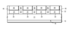
01 Growth of GaN on SiC substrates
Techniques for growing high-quality gallium nitride (GaN) layers on silicon carbide (SiC) substrates. SiC provides an excellent lattice-matched substrate for GaN epitaxial growth, resulting in reduced defect density and improved crystal quality. Various methods including MOCVD and MBE are used to deposit GaN on SiC wafers, often with buffer layers to minimize strain and improve interface quality.- Growth of GaN on SiC substrates: Silicon carbide (SiC) wafers serve as excellent substrates for the epitaxial growth of gallium nitride (GaN) layers due to their close lattice matching and high thermal conductivity. This combination allows for the production of high-quality GaN films with reduced defect densities. Various techniques such as MOCVD and MBE are employed to grow GaN on SiC substrates, enabling the fabrication of high-performance electronic and optoelectronic devices.
- SiC and GaN device fabrication techniques: Advanced fabrication techniques for silicon carbide and gallium nitride-based semiconductor devices involve specialized processing steps including wafer preparation, epitaxial growth, doping, etching, and metallization. These techniques address the challenges of working with wide bandgap materials and enable the production of high-performance electronic components such as transistors, diodes, and sensors with superior electrical properties for high-power, high-frequency, and high-temperature applications.
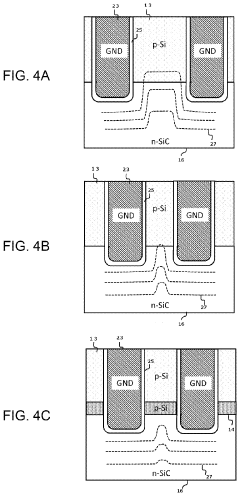
- Defect reduction in SiC and GaN materials: Methods for reducing crystallographic defects in silicon carbide wafers and gallium nitride films are critical for improving device performance and reliability. Techniques include specialized thermal treatments, buffer layer engineering, and surface preparation processes that minimize dislocations, micropipes, and other structural imperfections. These defect reduction strategies result in higher quality semiconductor materials suitable for advanced electronic applications.
- Heterostructure devices combining SiC and GaN: Heterostructure devices that combine silicon carbide and gallium nitride layers leverage the complementary properties of both materials to achieve superior performance. These structures typically feature GaN-based active regions on SiC substrates, enabling devices with enhanced thermal management, higher breakdown voltages, and improved reliability. Applications include high-electron-mobility transistors (HEMTs), power electronics, and RF devices operating under extreme conditions.
- Wafer bonding and transfer techniques for SiC and GaN: Wafer bonding and layer transfer technologies enable the integration of silicon carbide and gallium nitride materials with different substrate types. These techniques include direct wafer bonding, smart-cut processes, and engineered substrate approaches that facilitate the creation of composite wafer structures. Such methods overcome lattice mismatch limitations and thermal expansion differences, allowing for more versatile device architectures and improved performance in power electronics and optoelectronic applications.
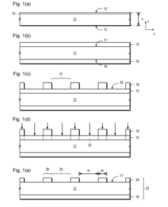
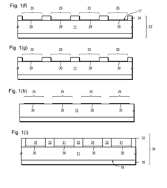
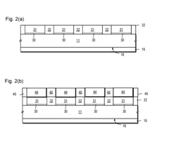
02 SiC wafer manufacturing and processing
Methods for manufacturing and processing silicon carbide wafers with improved quality and reduced defects. These include specialized cutting, polishing, and surface treatment techniques to prepare SiC wafers for subsequent device fabrication. Advanced processes address challenges such as micropipe defects, surface roughness, and wafer bow, resulting in higher quality substrates for power electronics and optoelectronic applications.Expand Specific Solutions03 GaN-on-SiC device structures
Semiconductor device structures utilizing gallium nitride layers on silicon carbide substrates. These include high-electron-mobility transistors (HEMTs), light-emitting diodes (LEDs), and power electronic devices. The combination leverages GaN's wide bandgap properties with SiC's thermal conductivity and structural compatibility to create high-performance electronic and optoelectronic devices with superior power handling and efficiency.Expand Specific Solutions04 Defect reduction in GaN/SiC interfaces
Techniques for reducing defects at the interface between gallium nitride and silicon carbide. These methods include specialized buffer layers, surface treatments, and growth parameter optimization to minimize lattice mismatch effects. Approaches such as AlN buffer layers, nucleation layers, and temperature-controlled growth sequences help reduce threading dislocations and other crystallographic defects that can propagate into the active device regions.Expand Specific Solutions05 Characterization and testing of SiC and GaN materials
Methods and systems for characterizing and testing silicon carbide wafers and gallium nitride layers. These include techniques for measuring crystal quality, defect density, electrical properties, and surface morphology. Advanced characterization tools such as X-ray diffraction, photoluminescence, and electrical measurements help evaluate material quality and predict device performance, enabling process optimization and quality control in manufacturing.Expand Specific Solutions
Key Industry Players in Wide Bandgap Semiconductor Market
The silicon carbide (SiC) and gallium nitride (GaN) wide bandgap semiconductor market is experiencing rapid growth, currently in the early mainstream adoption phase. The global market is projected to reach $4-5 billion by 2025, growing at a CAGR of 25-30%. Technologically, SiC is more mature with established manufacturing processes, while GaN is gaining momentum in high-frequency applications. Leading players include Wolfspeed, which dominates the SiC substrate market, Sumitomo Electric and RESONAC developing advanced wafer technologies, and Mitsubishi Electric and Infineon Technologies focusing on power device applications. Emerging competitors like MACOM and Power Integrations are accelerating GaN adoption, while research institutions such as University of Bath and Peking University are pioneering next-generation materials and fabrication techniques.
Wolfspeed, Inc.
Technical Solution: Wolfspeed is a global leader in silicon carbide (SiC) technology, offering a comprehensive portfolio of SiC wafers and devices. Their proprietary 150mm and 200mm SiC wafer manufacturing processes deliver industry-leading quality with defect densities below 1/cm². Wolfspeed's vertical integration approach encompasses the entire value chain from crystal growth to wafer fabrication, enabling tight quality control. Their SiC wafers feature micropipe densities <1/cm² and basal plane dislocations <1000/cm², significantly outperforming industry averages. Wolfspeed has demonstrated SiC MOSFETs operating at junction temperatures up to 200°C with switching frequencies exceeding 100kHz, compared to silicon's typical 150°C limit. Their latest generation SiC wafers show a 25% reduction in defect density while maintaining mechanical strength suitable for advanced device processing.
Strengths: Industry-leading SiC wafer quality with lowest defect densities; complete vertical integration from materials to devices; proven high-volume manufacturing capability. Weaknesses: Higher production costs compared to silicon; limited to SiC technology without significant GaN portfolio; manufacturing capacity constraints during industry-wide demand surges.
Sumitomo Electric Industries Ltd.
Technical Solution: Sumitomo Electric has pioneered advanced manufacturing techniques for both SiC and GaN substrates, with particular strength in GaN wafer technology. Their proprietary Vapor Phase Epitaxy (VPE) method produces GaN substrates with dislocation densities below 10⁶/cm², significantly lower than competing approaches. For SiC, they've developed a modified Physical Vapor Transport (PVT) process that reduces micropipe densities to near-zero levels while maintaining growth rates suitable for commercial production. Sumitomo's comparative analysis demonstrates their GaN substrates achieving thermal conductivity of 230 W/m·K versus 490 W/m·K for their SiC, but with superior electron mobility (1200 cm²/V·s vs 900 cm²/V·s for SiC). Their GaN substrates are available in diameters up to 6 inches with thickness uniformity of ±10μm, enabling next-generation power and RF devices. Sumitomo has also developed specialized polishing techniques that achieve surface roughness below 0.2nm RMS for both materials.
Strengths: Industry-leading GaN substrate quality; established production capabilities for both SiC and GaN; advanced epitaxial growth expertise for device-ready wafers. Weaknesses: Higher production costs compared to silicon-based alternatives; limited wafer diameter options compared to silicon; production capacity constraints for larger diameter GaN substrates.
Critical Patents and Technical Literature in WBG Materials
Power semiconductor device and method for manufacturing power semiconductor device
PatentInactiveUS20210119039A1
Innovation
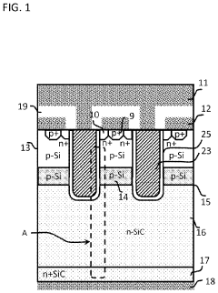
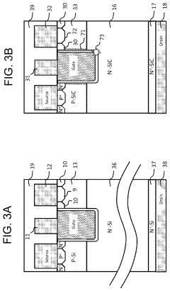
- A power semiconductor device structure is developed by directly bonding a SiC drift layer with a high bulk mobility onto a Si-MOSFET, incorporating trench gates and a block layer to enhance channel conduction and reduce electric field intrusion, thereby achieving low on-resistance and high breakdown voltage.
Gallium nitride on 3C—SiC composite wafer
PatentActiveUS9515222B2
Innovation
- A semiconductor structure is created with monocrystalline silicon carbide layers on a silicon wafer, interspersed with amorphous and/or polycrystalline silicon carbide layers, and monocrystalline and amorphous/polycrystalline gallium nitride layers, where the gallium nitride layers are grown in segments to neutralize stress across the wafer, reducing bow and mechanical deficiencies.
Supply Chain Resilience for Critical Semiconductor Materials
The global semiconductor supply chain faces significant vulnerabilities due to its reliance on critical materials like silicon carbide (SiC) and gallium nitride (GaN). These wide-bandgap semiconductors have become essential for next-generation power electronics, but their supply chains present distinct resilience challenges.
Silicon carbide wafer production is geographically concentrated, with major suppliers located in the United States, Japan, and Europe. The raw material processing requires specialized equipment and expertise, creating potential bottlenecks. Recent geopolitical tensions have highlighted vulnerabilities in this supply chain, as manufacturing capacity remains limited to a few key players like Wolfspeed, II-VI, and ROHM Semiconductor.
Gallium nitride faces different supply chain considerations. While gallium is more widely available as a byproduct of aluminum and zinc production, high-purity gallium suitable for semiconductor applications remains controlled by a small number of refiners, predominantly in China. This geographic concentration creates potential single points of failure in the supply chain.
Both materials face manufacturing challenges that impact supply chain resilience. SiC wafer production suffers from lower yields and higher defect rates compared to traditional silicon, limiting production scaling. GaN substrate availability remains constrained, with many manufacturers relying on heteroepitaxial growth on silicon or sapphire substrates, which introduces additional complexity.
Diversification strategies are emerging to enhance supply chain resilience. Major semiconductor companies are establishing redundant supplier relationships and investing in alternative sourcing regions. Government initiatives, particularly in the US and EU, are providing funding to develop domestic manufacturing capabilities for these critical materials through programs like the CHIPS Act.
Vertical integration is becoming increasingly important, with companies like STMicroelectronics and Infineon acquiring or partnering with raw material suppliers to secure their supply chains. This trend is more pronounced in the SiC ecosystem due to its manufacturing complexity.
Looking forward, recycling and material recovery programs represent an untapped opportunity to reduce supply chain vulnerabilities. Currently, end-of-life recovery rates for both SiC and GaN remain low, but developing circular economy approaches could significantly enhance long-term resilience while reducing environmental impact.
Environmental Impact and Sustainability Considerations
The environmental footprint of semiconductor materials has become increasingly important as the electronics industry faces growing scrutiny regarding sustainability. Silicon Carbide (SiC) and Gallium Nitride (GaN) present distinct environmental profiles throughout their lifecycle, from raw material extraction to end-of-life management.
SiC manufacturing requires extremely high temperatures (over 2000°C) for crystal growth, resulting in substantial energy consumption and associated carbon emissions. However, once deployed in applications, SiC devices demonstrate superior energy efficiency that can offset initial production impacts. The primary raw material, silicon, is abundant and has established recycling pathways, though carbon sources and processing chemicals present additional environmental considerations.
GaN production generally requires lower growth temperatures than SiC, potentially reducing energy requirements during manufacturing. However, gallium extraction presents unique environmental challenges as it is primarily obtained as a byproduct of aluminum and zinc processing, involving energy-intensive mining operations and potential habitat disruption. The limited global gallium supply also raises resource scarcity concerns.
Both materials offer significant sustainability advantages in application. Power electronics utilizing either SiC or GaN can achieve 30-50% energy savings compared to traditional silicon-based systems. In electric vehicles, these wide-bandgap semiconductors enable more efficient power conversion, extending range while reducing battery requirements and associated environmental impacts.
End-of-life considerations reveal important differences. SiC demonstrates exceptional chemical stability, presenting minimal leaching risk in landfills but also creating recycling challenges. GaN contains more valuable recoverable materials, potentially offering better economic incentives for recycling, though specialized processes are required to separate and purify these elements.
Water usage patterns differ significantly between the two technologies. SiC wafer production typically requires substantial water volumes for ingot slicing and polishing, while GaN manufacturing often employs molecular beam epitaxy or metal-organic chemical vapor deposition techniques with different water demand profiles. Recent innovations in both sectors have focused on closed-loop water systems to minimize consumption.
Regulatory landscapes increasingly favor materials with lower environmental impacts. The European Union's Restriction of Hazardous Substances (RoHS) directive and similar global regulations may influence future market dynamics for these materials, with manufacturers investing in cleaner production methods to maintain compliance and competitive advantage.
Unlock deeper insights with Patsnap Eureka Quick Research — get a full tech report to explore trends and direct your research. Try now!
Generate Your Research Report Instantly with AI Agent
Supercharge your innovation with Patsnap Eureka AI Agent Platform!