Designing Gate Drivers For Fast Switching SiC MOSFETs
SEP 8, 202510 MIN READ
Generate Your Research Report Instantly with AI Agent
Patsnap Eureka helps you evaluate technical feasibility & market potential.
SiC MOSFET Gate Driver Evolution and Objectives
Silicon Carbide (SiC) MOSFET technology has evolved significantly over the past two decades, transitioning from laboratory curiosity to commercial reality. The first commercial SiC Schottky diodes emerged in early 2000s, while SiC MOSFETs began gaining market traction around 2011 when Cree (now Wolfspeed) introduced their first generation devices. This technological progression has been driven by the inherent advantages of wide bandgap semiconductors over traditional silicon, including higher breakdown voltage, faster switching speeds, and superior thermal conductivity.
The evolution of SiC MOSFET gate drivers has followed a parallel but distinct trajectory, adapting to the unique requirements of these devices. Early gate drivers were essentially repurposed silicon IGBT drivers, which proved inadequate for exploiting SiC's full potential. The fundamental challenge stemmed from SiC MOSFETs' lower gate capacitance and higher switching speeds, which demanded more precise control mechanisms.
By 2015, specialized gate drivers began emerging with features specifically designed for SiC, including faster rise/fall times, negative bias capability, and improved common-mode transient immunity. The industry recognized that optimizing the gate driver was equally important as the SiC device itself for system performance. This realization sparked intensive research into advanced gate driving techniques.
Recent developments have focused on intelligent gate drivers incorporating adaptive control algorithms, real-time monitoring, and protection features. These sophisticated drivers can dynamically adjust gate resistance, voltage levels, and switching profiles based on operating conditions, significantly enhancing system reliability while maximizing switching performance.
The primary objective of modern SiC MOSFET gate driver design is to achieve an optimal balance between switching speed and system reliability. Faster switching reduces losses but increases electromagnetic interference (EMI) and voltage overshoots that can compromise system integrity. This fundamental trade-off defines the central challenge in gate driver development.
Additional objectives include improving immunity to parasitic turn-on effects, enhancing short-circuit protection capabilities, and developing cost-effective isolation solutions capable of withstanding the high dv/dt rates inherent to SiC operation. Temperature compensation has also emerged as a critical goal, as SiC devices exhibit different switching characteristics across their wide operating temperature range.
Looking forward, the industry is moving toward greater integration of gate drivers with power modules, incorporating advanced sensing and protection features directly into the package. The ultimate goal is to develop "plug-and-play" SiC power solutions that simplify system design while maximizing performance and reliability, thereby accelerating SiC adoption across automotive, renewable energy, and industrial applications.
Market Demand Analysis for Fast Switching SiC Applications
The Silicon Carbide (SiC) MOSFET market is experiencing unprecedented growth, driven primarily by the global shift towards electrification and energy efficiency. Current market analyses indicate that the SiC power device market is expanding at a CAGR of 30% and is projected to reach $3 billion by 2025. This rapid growth trajectory is creating substantial demand for specialized gate drivers capable of handling the unique switching characteristics of SiC MOSFETs.
The automotive sector represents the largest application segment for fast-switching SiC MOSFETs, accounting for approximately 45% of the total market. Electric vehicle manufacturers are increasingly adopting SiC technology in their traction inverters, onboard chargers, and DC-DC converters to achieve higher power density, improved efficiency, and extended driving range. Industry reports suggest that a SiC-based powertrain can improve an EV's range by up to 10% compared to traditional silicon-based systems.
Industrial applications constitute the second-largest market segment at 30%, with particular demand in motor drives, solar inverters, and uninterruptible power supplies. The ability of SiC MOSFETs to operate at higher frequencies enables smaller passive components, resulting in more compact and efficient power conversion systems. This characteristic is especially valuable in space-constrained industrial environments where power density is paramount.
The renewable energy sector is emerging as a rapidly growing application area, currently representing 15% of the market but expanding at a faster rate than other segments. Solar inverters and wind power converters benefit significantly from SiC technology's higher efficiency, which translates directly into increased energy harvest and improved return on investment for renewable installations.
Market research indicates that end-users are willing to pay a premium of 20-30% for SiC-based solutions compared to traditional silicon alternatives, provided they deliver tangible performance improvements. This price tolerance is creating a favorable environment for innovation in gate driver technology, as manufacturers can justify R&D investments with the promise of higher margins.
Regional analysis shows North America and Europe leading SiC adoption, collectively accounting for 65% of the global market. However, Asia-Pacific, particularly China, is investing heavily in SiC manufacturing capabilities and is expected to show the highest growth rate over the next five years. This geographic distribution is influencing the supply chain dynamics for gate driver components, with many manufacturers establishing regional production facilities to serve local markets efficiently.
Customer requirements are evolving rapidly, with increasing emphasis on gate drivers that can support switching frequencies above 100 kHz while maintaining robust protection features. Survey data from power electronics engineers indicates that 78% consider gate driver performance a critical factor in their SiC MOSFET selection process, highlighting the interconnected nature of these components in system design.
Technical Challenges in SiC MOSFET Gate Driver Design
Silicon Carbide (SiC) MOSFETs represent a significant advancement in power semiconductor technology, offering superior performance compared to traditional silicon-based devices. However, their implementation presents unique challenges, particularly in gate driver design. The high switching speeds of SiC MOSFETs, while advantageous for efficiency, create complex requirements for gate drivers that must be carefully addressed.
One of the primary challenges is managing the significantly higher switching speeds. SiC MOSFETs can switch at rates up to 100 kV/μs, which is substantially faster than silicon counterparts. This rapid switching creates severe electromagnetic interference (EMI) issues that can affect system reliability and performance. Gate drivers must incorporate advanced EMI mitigation techniques, including optimized PCB layouts, strategic component placement, and effective shielding methodologies.
The gate voltage requirements for SiC MOSFETs present another significant challenge. Unlike silicon devices that typically operate with gate voltages of +15V/-5V, SiC MOSFETs often require +20V/-5V or even higher positive voltages to achieve optimal performance. This necessitates specialized gate driver designs capable of delivering these voltage levels consistently and reliably, while also protecting against overvoltage conditions that could damage the sensitive gate oxide.
Parasitic inductance management represents a critical technical hurdle in SiC MOSFET gate driver design. The high dv/dt and di/dt characteristics of these devices make them particularly susceptible to parasitic inductances in the gate drive loop. These inductances can cause voltage oscillations, gate ringing, and potentially destructive voltage spikes. Minimizing loop inductance through careful PCB layout and component selection becomes essential for stable operation.
Temperature sensitivity adds another layer of complexity. SiC MOSFETs exhibit different threshold voltage characteristics across temperature ranges compared to silicon devices. Gate drivers must compensate for these variations to maintain consistent switching performance across the entire operating temperature range, which is particularly challenging in automotive and industrial applications where temperature fluctuations are common.
The isolation requirements for gate drivers in SiC MOSFET applications are also more demanding. The higher blocking voltages of SiC devices (often exceeding 1200V) necessitate robust isolation between the control circuitry and the power stage. This requires advanced isolation technologies with higher common-mode transient immunity (CMTI) ratings, typically exceeding 100 kV/μs, to prevent false triggering during high-speed switching events.
Short-circuit protection mechanisms must be redesigned for SiC MOSFETs due to their different characteristics. The traditional desaturation detection methods used for silicon IGBTs may not be fast enough for SiC MOSFETs, which can reach destructive current levels within nanoseconds during fault conditions. Advanced protection schemes with response times under 200ns are necessary to safeguard these expensive components.
Current Gate Driver Solutions for SiC MOSFETs
01 High-speed gate driver designs for SiC MOSFETs
Specialized gate driver designs that can handle the fast switching capabilities of SiC MOSFETs. These designs incorporate optimized circuit topologies to minimize switching losses and improve efficiency. Features include reduced parasitic inductance, enhanced dv/dt immunity, and precise timing control to enable the full performance potential of SiC devices in high-frequency applications.- High-speed gate driver designs for SiC MOSFETs: Specialized gate driver designs that enable fast switching of Silicon Carbide (SiC) MOSFETs while minimizing switching losses. These designs incorporate optimized gate resistors, advanced layout techniques, and high-frequency components to handle the rapid dv/dt and di/dt rates characteristic of SiC devices. The drivers provide precise control of turn-on and turn-off times to maximize efficiency while preventing voltage overshoots and ringing.
- Isolated gate driver solutions for SiC power modules: Gate driver solutions that provide galvanic isolation between the control circuitry and the high-voltage SiC power stage. These designs incorporate isolation technologies such as optocouplers, transformers, or digital isolators to maintain signal integrity while protecting the control system. The isolated drivers deliver sufficient current and voltage to rapidly switch SiC MOSFETs while maintaining immunity to common-mode transients that occur during fast switching events.
- Temperature-compensated gate driving techniques: Gate driving techniques that adjust parameters based on operating temperature to maintain optimal switching performance of SiC MOSFETs across varying conditions. These solutions incorporate temperature sensing and adaptive control to modify gate voltage levels, slew rates, or dead-time periods. By compensating for the temperature-dependent characteristics of SiC devices, these drivers ensure consistent switching behavior and prevent thermal runaway during high-speed operation.
- Multi-level and asymmetric gate driving for SiC devices: Advanced gate driving techniques that employ different voltage levels or asymmetric profiles during turn-on and turn-off transitions of SiC MOSFETs. These approaches use positive and negative bias voltages with optimized timing to enhance switching speed while reducing losses and electromagnetic interference. The drivers may incorporate separate paths for charging and discharging the gate, allowing independent control of rising and falling edges to balance switching speed against ringing and overshoot concerns.
- Integrated protection features for SiC gate drivers: Gate driver designs with built-in protection mechanisms specifically tailored for the high-speed switching characteristics of SiC MOSFETs. These drivers incorporate features such as desaturation detection, overcurrent protection, short-circuit protection, and under-voltage lockout with response times fast enough for SiC applications. Advanced designs may include active clamping circuits to limit voltage spikes during switching transients and soft shutdown capabilities to safely handle fault conditions without device damage.
02 Gate drive isolation techniques for SiC applications
Isolation methods specifically designed for SiC MOSFET gate drivers to maintain signal integrity during high-speed switching. These techniques include galvanic isolation using transformers, optocouplers, or capacitive coupling to protect control circuitry from high voltages while maintaining fast response times. Advanced isolation barriers help prevent common-mode noise issues that can affect the reliable operation of SiC-based power converters.Expand Specific Solutions03 Adaptive gate driving methods for SiC MOSFETs
Intelligent gate driving techniques that dynamically adjust gate parameters based on operating conditions. These methods include variable gate resistance, multi-level gate voltage control, and active gate driving to optimize switching behavior. By adapting to changing load and temperature conditions, these systems can balance switching speed with EMI generation and ensure reliable operation across the entire operating range of SiC devices.Expand Specific Solutions04 Integrated protection features for SiC gate drivers
Protection mechanisms integrated into gate driver circuits to safeguard SiC MOSFETs during fast switching events. These features include overcurrent protection, short-circuit detection, under-voltage lockout, and temperature monitoring. Advanced protection schemes can respond within nanoseconds to prevent device failure while maintaining the high-speed switching capability that makes SiC devices advantageous.Expand Specific Solutions05 Gate driver power supply optimization for SiC devices
Specialized power supply designs for gate drivers that can deliver the precise voltage levels and current requirements needed for optimal SiC MOSFET switching. These designs feature low-impedance paths, local energy storage, and regulated voltage supplies to ensure clean gate signals. Proper power supply design is critical for maintaining consistent gate voltage during high-frequency operation and preventing gate oscillations that can lead to device failure.Expand Specific Solutions
Key Industry Players in SiC MOSFET and Gate Driver Market
The SiC MOSFET gate driver market is in a growth phase, driven by increasing demand for high-efficiency power conversion systems. The market is expanding rapidly with a projected CAGR of 25-30% as industries transition to wide bandgap semiconductors. Technologically, the field is maturing but still evolving, with companies developing specialized solutions for the unique challenges of fast switching SiC devices. Key players include established power semiconductor manufacturers like Microchip Technology, Power Integrations, ROHM, and Mitsubishi Electric, who are competing with newer entrants from China such as Global Power Technology and Suzhou Convert Semiconductor. Academic institutions including North Carolina State University and University of Electronic Science & Technology of China are contributing significant research to advance gate driver technology for higher switching speeds and improved reliability.
Microchip Technology, Inc.
Technical Solution: Microchip has developed the AgileSwitch® gate driver technology specifically for SiC MOSFETs, featuring Augmented Switching™ technology that provides precise control over switching waveforms. Their solution implements digital configurability of gate drive parameters including turn-on/off speeds, dead time, and undervoltage lockout thresholds, allowing optimization for specific application requirements. The gate drivers incorporate advanced Active Miller Clamping with programmable clamp strength and duration, effectively suppressing unwanted turn-on events during high dv/dt transients. Microchip's SiC gate drivers feature integrated temperature monitoring and compensation circuits that automatically adjust drive parameters as operating conditions change, maintaining optimal switching performance across temperature ranges. Their technology includes Fault Management and Reporting features with configurable responses to short circuits, overcurrent, and overtemperature conditions, providing comprehensive protection while maintaining high system availability.
Strengths: Highly configurable digital control interface allows precise tuning of switching parameters without hardware changes. Comprehensive telemetry and fault reporting capabilities enhance system monitoring and diagnostics. Weaknesses: More complex implementation requiring digital configuration tools, and potentially higher initial cost compared to analog solutions.
Power Integrations, Inc.
Technical Solution: Power Integrations has developed the SCALE-iDriver family specifically engineered for SiC MOSFETs, featuring FluxLink™ technology that provides reinforced isolation without optocouplers or transformers. Their gate drivers deliver peak output currents up to 8A with programmable turn-on and turn-off strengths to optimize switching performance. The architecture incorporates Advanced Active Clamping (AAC) that protects against voltage overshoots during switching transients by dynamically adjusting the gate voltage. Their SiC MOSFET drivers include integrated Advanced Soft-Shutdown (ASS) technology that provides controlled shutdown during fault conditions, preventing voltage spikes while maintaining fast response times. Power Integrations' solutions feature built-in undervoltage lockout (UVLO), overvoltage protection, and short-circuit protection with response times under 500ns, addressing the critical protection requirements of SiC MOSFETs operating at high switching frequencies.
Strengths: FluxLink™ technology provides superior isolation performance with lower coupling capacitance compared to optocoupler solutions, enabling faster switching speeds. Integrated protection features simplify system design and enhance reliability. Weaknesses: Limited configurability in some product lines compared to discrete solutions, and potentially higher implementation costs for low-volume applications.
Critical Patents and Innovations in SiC Gate Driver Design
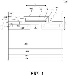
High temperature gate driver for silicon carbide metal-oxide-semiconductor field-effect transistor
PatentActiveUS11218145B2
Innovation
- A low-cost high temperature gate driver utilizing commercial-off-the-shelf discrete transistors and diodes, integrated with a robust overcurrent and under voltage lock out protection circuit, capable of operating up to 180°C, featuring a reduced propagation delay and flexible short-circuit protection, designed to minimize self-heating and enhance reliability.
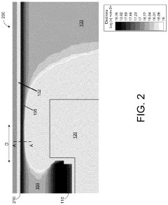
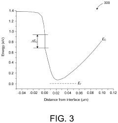
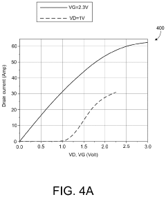
Silicon carbide field-effect transistors
PatentActiveUS11894454B2
Innovation
- The development of a silicon carbide (SiC) metal-oxide-semiconductor field-effect transistor (MOSFET) with a gate structure comprising a gate oxide layer, an aluminum nitride layer, and a p-type gallium nitride layer, which includes a lateral built-in channel with a p-type AlGaN gate and an AlN buffer layer, providing high threshold voltage and low interface trap density, enabling efficient operation with low on-state resistance.
Thermal Management Strategies for High-Frequency Operation
The thermal management of SiC MOSFET gate drivers operating at high frequencies presents unique challenges that require specialized solutions. As switching frequencies increase, power losses in both the gate driver circuitry and the SiC MOSFET itself generate significant heat that must be effectively dissipated to maintain reliable operation and prevent thermal runaway conditions.
Heat generation in high-frequency operation primarily stems from switching losses, which increase proportionally with frequency. The gate driver IC itself becomes a notable heat source when operating at frequencies exceeding 100 kHz, with power dissipation typically ranging from 2-5W depending on the gate charge requirements and switching speed.
Effective thermal management strategies begin at the PCB design level. Multi-layer PCBs with dedicated thermal planes and strategically placed thermal vias can significantly enhance heat dissipation from both the gate driver IC and surrounding components. For optimal thermal performance, the thermal resistance path should be minimized by placing thermal vias directly under heat-generating components and connecting to inner copper planes.
Advanced cooling techniques become necessary as frequencies push beyond 500 kHz. These include forced-air cooling with optimized heatsink designs, liquid cooling systems for extreme high-power applications, and phase-change materials that provide thermal buffering during transient high-power operation. Recent innovations in thermally conductive polymers and ceramic substrates offer promising alternatives to traditional aluminum heatsinks, providing up to 30% improvement in thermal conductivity while reducing weight.
Temperature monitoring and dynamic thermal management represent another critical aspect of high-frequency operation. Integrating temperature sensors near gate driver ICs allows for real-time monitoring and implementation of protective measures such as dynamic frequency reduction or shutdown procedures when thermal thresholds are exceeded. Advanced gate drivers now incorporate built-in temperature sensing and protection features that can adjust driving parameters based on thermal conditions.
The physical layout of components also plays a crucial role in thermal management. Creating thermal isolation zones between high-temperature components prevents heat concentration and reduces thermal coupling effects. Careful consideration of component placement can create natural convection pathways that enhance passive cooling efficiency by up to 25%.
Emerging technologies such as embedded cooling channels within PCB substrates and direct die-attach methods are showing promising results for next-generation high-frequency SiC MOSFET applications, potentially enabling operation at frequencies exceeding 1 MHz while maintaining junction temperatures below critical thresholds.
EMI Mitigation Techniques for SiC-Based Power Systems
Electromagnetic Interference (EMI) has emerged as a critical challenge in SiC MOSFET-based power systems due to the inherently fast switching speeds these devices achieve. The high dv/dt and di/dt rates, while beneficial for efficiency, generate significant electromagnetic noise that can compromise system reliability and regulatory compliance. Effective EMI mitigation requires a multi-faceted approach addressing both conducted and radiated emissions.
Gate driver design plays a pivotal role in EMI management for SiC MOSFETs. Implementing active gate driving techniques allows for precise control of switching transitions, effectively reducing EMI at its source. Techniques such as variable gate resistance, multi-level gate voltage profiles, and closed-loop current control can shape switching waveforms to minimize oscillations while maintaining acceptable switching losses.
Layout optimization represents another crucial EMI mitigation strategy. Minimizing gate loop and power loop inductances through careful PCB design significantly reduces ringing and associated emissions. Strategic component placement, with special attention to decoupling capacitors and gate driver positioning, can substantially attenuate noise propagation paths. The implementation of Kelvin source connections further reduces common-source inductance, a major contributor to switching oscillations.
Shielding and filtering constitute essential supplementary measures for comprehensive EMI management. Common mode chokes, Y-capacitors, and ferrite beads strategically placed in power and signal paths can attenuate conducted emissions across specific frequency bands. For high-frequency radiated emissions, proper shielding enclosures and grounding schemes prevent interference from affecting sensitive components or adjacent systems.
Advanced modulation strategies offer system-level approaches to EMI reduction. Techniques such as spread spectrum modulation distribute switching energy across a wider frequency range, reducing peak emissions at any single frequency. Similarly, interleaving multiple power stages can lead to partial EMI cancellation effects, particularly beneficial in multi-phase converter topologies.
Simulation and predictive modeling have become increasingly important in EMI mitigation. Parasitic extraction tools coupled with circuit and electromagnetic field simulators enable engineers to predict EMI issues before physical prototyping. These virtual prototyping approaches allow for iterative optimization of layout, component selection, and filtering strategies, significantly reducing development cycles and compliance issues.
Standardized testing methodologies ensure that implemented EMI mitigation techniques meet regulatory requirements. Conducted emission tests using Line Impedance Stabilization Networks (LISN) and radiated emission measurements in anechoic chambers provide quantitative validation of mitigation effectiveness across the regulated frequency spectrum.
Unlock deeper insights with Patsnap Eureka Quick Research — get a full tech report to explore trends and direct your research. Try now!
Generate Your Research Report Instantly with AI Agent
Supercharge your innovation with Patsnap Eureka AI Agent Platform!