EUV Lithography: Innovations and Intellectual Property Challenges
OCT 14, 20259 MIN READ
Generate Your Research Report Instantly with AI Agent
Patsnap Eureka helps you evaluate technical feasibility & market potential.
EUV Lithography Evolution and Objectives
Extreme Ultraviolet (EUV) lithography represents a revolutionary advancement in semiconductor manufacturing technology, marking a significant departure from traditional optical lithography methods. The evolution of EUV technology spans several decades, beginning in the 1980s with initial research into short-wavelength lithography techniques. By the 1990s, EUV emerged as a promising candidate for next-generation lithography, utilizing 13.5nm wavelength light to enable the production of increasingly miniaturized semiconductor components.
The development trajectory accelerated in the early 2000s when industry consortia like ASML, Intel, and Samsung began substantial investments in EUV research. A critical milestone occurred in 2006 with the demonstration of the first full-field EUV exposure tools, though significant technical challenges remained. The period between 2010 and 2018 saw intensive engineering efforts to overcome issues related to source power, mask defects, and throughput limitations.
Commercial viability was finally achieved in 2019 when ASML delivered production-ready EUV lithography systems to leading semiconductor manufacturers, enabling high-volume manufacturing at the 7nm node and below. This breakthrough represented the culmination of over $15 billion in research and development investment across the industry.
The primary objective of EUV lithography technology is to extend Moore's Law by enabling the continued miniaturization of semiconductor devices. Specifically, EUV aims to facilitate mass production of integrated circuits with feature sizes below 10nm while maintaining economic viability. This involves achieving sufficient throughput, yield, and cost-effectiveness to support high-volume manufacturing operations.
Secondary objectives include reducing multi-patterning requirements that had become necessary with previous lithography techniques, thereby simplifying the manufacturing process and potentially reducing costs. EUV technology also aims to improve pattern fidelity and reduce edge placement errors, critical factors in advanced semiconductor performance.
Looking forward, the technology roadmap for EUV lithography includes the development of high-numerical-aperture (high-NA) EUV systems, targeting resolution improvements of approximately 70% to enable 3nm node production and beyond. Additional objectives include enhancing source power to exceed 500W, improving mask infrastructure to reduce defectivity, and developing more sensitive photoresists with improved line-edge roughness characteristics.
The evolution of EUV technology continues to be driven by the semiconductor industry's relentless pursuit of higher performance, lower power consumption, and increased functionality in electronic devices, establishing new paradigms for manufacturing capabilities while presenting unique intellectual property challenges as the technology matures.
Semiconductor Industry Demand for EUV Technology
The semiconductor industry's demand for Extreme Ultraviolet (EUV) lithography technology has been driven by the relentless pursuit of Moore's Law, which predicts the doubling of transistor density approximately every two years. As conventional deep ultraviolet (DUV) lithography approaches its physical limits around the 7nm node, EUV has emerged as the critical enabler for continued miniaturization in advanced semiconductor manufacturing.
Market research indicates that the global semiconductor industry, valued at over $550 billion, is increasingly dependent on EUV technology to maintain its growth trajectory. The demand is particularly acute in the high-performance computing, mobile, artificial intelligence, and automotive sectors, where chip performance and power efficiency requirements continue to escalate. Leading foundries and integrated device manufacturers have committed billions in capital expenditure specifically for EUV implementation.
The economic drivers behind EUV adoption are compelling despite its high implementation costs. While an EUV lithography system represents a capital investment exceeding $150 million per unit, manufacturers recognize that the technology enables critical dimension uniformity and pattern fidelity that are unachievable with multiple DUV patterning steps. This translates to higher yields, reduced process complexity, and ultimately lower cost-per-transistor for advanced nodes below 7nm.
Geographically, the demand for EUV technology is concentrated in East Asia, particularly Taiwan, South Korea, and increasingly China, where the majority of advanced semiconductor manufacturing occurs. North America and Europe maintain significant demand through their research institutions and specialized semiconductor manufacturers focusing on cutting-edge applications.
Industry forecasts project the EUV lithography equipment market to grow at a compound annual growth rate of 21% through 2026, reflecting the technology's transition from early adoption to mainstream implementation. This growth is supported by the expanding application scope beyond logic chips to include advanced memory production, particularly for high-bandwidth memory (HBM) and advanced DRAM technologies.
The demand is further intensified by geopolitical factors and national semiconductor strategies. Multiple countries have established initiatives to secure domestic advanced semiconductor manufacturing capabilities, with EUV technology recognized as a strategic asset. This has created additional market pressure and competition for limited EUV system supply, with delivery times extending to over 18 months for new systems.
Customer requirements are evolving beyond basic EUV implementation to demand higher numerical aperture EUV systems (High-NA EUV), which promise to extend scaling capabilities to the 2nm node and beyond, ensuring continued market growth for this technology through the next decade.
EUV Technical Barriers and Global Development Status
Extreme Ultraviolet (EUV) lithography represents a revolutionary advancement in semiconductor manufacturing, yet faces significant technical barriers that have influenced its global development trajectory. The primary technical challenge remains the EUV light source, which requires generating and maintaining plasma at temperatures exceeding 200,000°C to produce 13.5nm wavelength light. This process demands substantial energy input while yielding only 2-3% conversion efficiency, creating significant thermal management challenges and reliability issues.
Photomask defectivity presents another critical barrier. EUV masks utilize complex multilayer reflective structures rather than traditional transmissive designs, making defect detection and repair substantially more difficult. Even nanometer-scale defects can cause catastrophic pattern failures, necessitating unprecedented levels of cleanliness and inspection capabilities.
Photoresist technology continues to challenge manufacturers, as EUV resists must simultaneously achieve high resolution, low line edge roughness, and sufficient sensitivity—a combination known as the "triangle trade-off" that has proven difficult to optimize. Current resists struggle to balance these competing requirements while maintaining manufacturing viability.
From a global development perspective, EUV technology exhibits distinct geographical concentration. The Netherlands-based ASML maintains a virtual monopoly on EUV lithography systems, creating significant geopolitical implications. The United States and Japan supply critical components, while South Korea and Taiwan represent the primary adopters implementing the technology at scale.
China's access to EUV technology has been restricted through export controls, creating a bifurcated development landscape. Leading semiconductor manufacturers in Taiwan (TSMC) and South Korea (Samsung) have successfully integrated EUV into high-volume manufacturing for 7nm nodes and beyond, while Chinese manufacturers must pursue alternative approaches for advanced node production.
The economic barriers to EUV adoption remain substantial. Each EUV lithography system costs approximately $150-200 million, with significant additional infrastructure requirements. This has limited adoption to only the largest semiconductor manufacturers, reinforcing industry consolidation trends and widening the technological gap between leading-edge and trailing manufacturers.
Despite these challenges, EUV development continues to advance globally, with ASML and its partners pursuing higher numerical aperture systems (High-NA EUV) to enable future nodes below 3nm. The technology's trajectory remains heavily influenced by the complex interplay of technical barriers, geopolitical factors, and economic considerations that have shaped its development since inception.
Current EUV Implementation Approaches
01 EUV Lithography System Innovations
Innovations in EUV lithography systems focus on improving the optical components, light sources, and overall system architecture to enhance resolution and performance. These innovations include advanced mirror designs, illumination systems, and integration of components to achieve higher throughput and better image quality. The systems are designed to handle the unique challenges of extreme ultraviolet wavelengths while maintaining precision in semiconductor manufacturing processes.- EUV Lithography System Innovations: Innovations in EUV lithography systems focus on improving the optical components, light sources, and overall system architecture to enhance resolution and performance. These innovations include advanced mirror designs, illumination systems, and integration of components to achieve higher precision and throughput in semiconductor manufacturing. The systems are designed to work with extreme ultraviolet light to pattern semiconductor wafers at nanometer scales.
- Mask and Reticle Technology for EUV: Advancements in mask and reticle technology are critical for EUV lithography. These innovations include reflective mask designs, defect inspection and repair methods, and pattern optimization techniques. The masks are engineered to precisely control the reflection of EUV light to create the desired patterns on semiconductor wafers with minimal defects and maximum accuracy.
- EUV Resist Materials and Processing: Development of specialized resist materials and processing techniques for EUV lithography addresses challenges such as sensitivity, resolution, and line edge roughness. These innovations include chemical amplification mechanisms, post-exposure bake processes, and development techniques that enhance pattern transfer accuracy while minimizing defects. Advanced resist formulations are designed to respond optimally to the specific wavelength of EUV radiation.
- Intellectual Property Management for EUV Technology: Intellectual property strategies specific to EUV lithography include patent portfolio management, licensing frameworks, and collaborative development agreements. These approaches address the complex ecosystem of EUV technology development, where multiple companies contribute different components and subsystems. IP management systems help navigate the dense patent landscape while facilitating technology advancement through strategic partnerships and cross-licensing.
- Contamination Control and System Reliability: Innovations addressing contamination control and system reliability in EUV lithography focus on maintaining clean operating environments, managing thermal effects, and ensuring consistent performance. These technologies include advanced vacuum systems, particle mitigation strategies, and thermal management solutions that protect sensitive optical components from degradation. Monitoring systems track performance metrics to maintain production quality over extended operation periods.
02 Mask and Reticle Technology for EUV
Advancements in mask and reticle technology are crucial for EUV lithography. These innovations include specialized materials and structures that can effectively pattern EUV light, methods to reduce defects in masks, and techniques to enhance pattern fidelity. The development of reflective masks specifically designed for EUV wavelengths has been a significant area of innovation, along with inspection and repair technologies to ensure mask quality.Expand Specific Solutions03 EUV Resist and Materials Development
The development of specialized photoresist materials and other materials for EUV lithography has been a key area of innovation. These materials are designed to be highly sensitive to EUV radiation while providing high resolution, low line edge roughness, and good etch resistance. Innovations include chemical amplification mechanisms, metal-containing resists, and multi-layer material stacks that enhance the performance of EUV lithography processes.Expand Specific Solutions04 EUV Process Control and Optimization
Innovations in process control and optimization for EUV lithography focus on methods to enhance yield, reliability, and consistency in semiconductor manufacturing. These include advanced metrology techniques, computational models for process simulation, and feedback systems that can adjust process parameters in real-time. The development of specialized software tools and algorithms to optimize EUV exposure conditions and pattern transfer has been critical for the industrial implementation of this technology.Expand Specific Solutions05 Intellectual Property Management for EUV Technology
The management of intellectual property related to EUV lithography has become increasingly important as the technology matures. Innovations in this area include methods for valuing and trading EUV-related patents, strategies for building and maintaining patent portfolios, and approaches to licensing technology across the semiconductor ecosystem. These innovations help companies navigate the complex IP landscape of EUV lithography while protecting their investments in research and development.Expand Specific Solutions
Leading Companies in EUV Lithography Ecosystem
EUV Lithography is currently in a growth phase, with the market expected to expand significantly due to increasing demand for advanced semiconductor manufacturing. The technology has reached commercial viability but continues to evolve rapidly. ASML Netherlands BV dominates the EUV equipment market as the sole supplier of production-ready EUV lithography systems. Leading semiconductor manufacturers like Taiwan Semiconductor Manufacturing Co., Intel, and Samsung SDI are driving adoption, investing heavily in EUV implementation. Supporting ecosystem players including Shin-Etsu Chemical, Tokyo Electron, and Lam Research provide critical materials and complementary equipment. The intellectual property landscape is highly competitive, with major players building extensive patent portfolios to protect their innovations in this strategically important technology that enables continued semiconductor scaling.
Taiwan Semiconductor Manufacturing Co., Ltd.
Technical Solution: TSMC has pioneered the implementation of EUV lithography in high-volume manufacturing, beginning with their 7nm+ process and expanding to 5nm and 3nm nodes. Their EUV implementation strategy involves a hybrid approach that selectively applies EUV to critical layers while using immersion lithography for less demanding layers, optimizing cost-performance balance[1]. TSMC has developed proprietary computational lithography techniques that enhance EUV pattern fidelity through optical proximity correction and source mask optimization. Their process integrates specialized EUV resists co-developed with suppliers that achieve high sensitivity while maintaining resolution and line edge roughness requirements[2]. TSMC has implemented innovative solutions for EUV mask defect inspection and repair, critical for maintaining yield in high-volume manufacturing. Their EUV implementation includes advanced process control systems that compensate for variations in the EUV source power and stability, ensuring consistent patterning across wafers[3].
Strengths: Industry-leading implementation of EUV in high-volume manufacturing; extensive process integration expertise; strong collaboration with equipment and materials suppliers. Weaknesses: Heavy dependence on ASML for equipment; high capital expenditure requirements; geopolitical vulnerabilities due to concentration of advanced manufacturing.
SAMSUNG SDI CO LTD
Technical Solution: Samsung has implemented EUV lithography extensively in their semiconductor manufacturing, beginning with their 7nm process node. Their approach includes a proprietary multi-patterning scheme that optimizes the balance between EUV and conventional lithography steps to manage cost while achieving required resolution[1]. Samsung has developed specialized EUV process integration techniques that address the challenges of etching EUV-patterned features with high fidelity. Their implementation includes innovative approaches to stochastic defect mitigation through design rule optimization and computational correction[2]. Samsung has created proprietary solutions for EUV mask infrastructure, including advanced inspection and repair capabilities critical for high-volume manufacturing. Their EUV implementation strategy includes specialized process control methods that compensate for variations in EUV source power and stability[3]. Samsung has also invested significantly in research for next-generation High-NA EUV technology, positioning themselves for future technology nodes.
Strengths: Vertically integrated business model from equipment research to chip design; strong memory-specific EUV implementation expertise; extensive manufacturing scale. Weaknesses: Higher dependence on external technology partners compared to TSMC; challenges in logic process competitiveness; high capital requirements for maintaining technology parity.
Critical Patents and Technical Innovations in EUV
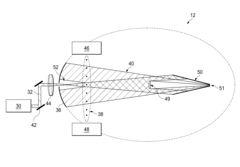
Extreme ultraviolet lithography device and method of operating extreme ultraviolet lithography device
PatentActiveUS11960212B2
Innovation
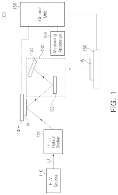
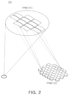
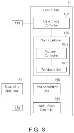
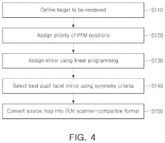
- The implementation of a freeform EUV illumination system using linear programming and priority optimization to assign mirror positions, allowing for the generation of an optimized illumination system that can be converted into a form recognizable by an EUV scanner, thereby improving patterning performance.
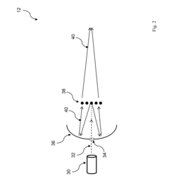
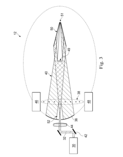
Collector in an Extreme Ultraviolet Lithography System with Optimal Air Curtain Protection
PatentActiveUS20160306282A1
Innovation
- An EUV radiation source with a collector module integrated gas supply mechanism forms an air curtain using hydrogen gas, creating a protective layer on the collector surface and a purge cone to prevent contamination, utilizing a supply gap and gas pipeline with inward and outward entrances to ensure comprehensive coverage.
Intellectual Property Landscape and Legal Challenges
The intellectual property landscape surrounding EUV lithography is characterized by dense patent thickets and complex cross-licensing agreements among major industry players. ASML, the sole manufacturer of commercial EUV lithography systems, holds a dominant position with over 2,000 patents specifically related to EUV technology. This concentration of IP rights creates significant barriers to entry for potential competitors and raises concerns about market monopolization.
Patent disputes in the EUV domain frequently center on critical components such as light sources, mirrors, and photoresist technologies. Notable litigation cases include the 2019 dispute between ASML and Nikon regarding optical alignment systems, which was eventually settled through a cross-licensing agreement valued at approximately $150 million. Such settlements highlight the high financial stakes involved in EUV intellectual property.
The international dimension of EUV IP protection presents additional challenges. Export control regulations, particularly those implemented by the United States and the Netherlands, restrict the transfer of EUV technology to certain countries, creating geopolitical tensions and potentially fragmenting the global semiconductor supply chain. These restrictions have significant implications for technology access and national competitiveness in advanced semiconductor manufacturing.
Standard-essential patents (SEPs) represent another critical aspect of the EUV IP landscape. Industry consortia like SEMI and SEMATECH have established technical standards that incorporate patented technologies, necessitating complex licensing frameworks to ensure both fair access and appropriate compensation for innovation. The determination of FRAND (Fair, Reasonable, And Non-Discriminatory) licensing terms remains contentious among industry stakeholders.
Open innovation initiatives are emerging as potential solutions to IP bottlenecks. Research collaborations between semiconductor manufacturers, equipment suppliers, and academic institutions aim to develop pre-competitive technologies that can be broadly licensed. The IMEC research center in Belgium exemplifies this approach, creating shared IP pools that facilitate technology advancement while reducing legal barriers.
Looking forward, the evolution of IP strategies in the EUV ecosystem will likely involve increased emphasis on defensive patent portfolios and strategic alliances. Companies are increasingly focusing on securing patents not only for their core innovations but also for adjacent technologies that could provide competitive advantages or bargaining power in licensing negotiations. This trend toward broader patent coverage may further complicate the IP landscape while simultaneously creating opportunities for novel licensing and collaboration models.
Supply Chain Security and Geopolitical Implications
The global supply chain for EUV lithography represents one of the most complex and strategically significant technological ecosystems in the semiconductor industry. ASML, the Dutch company that holds a virtual monopoly on EUV lithography systems, relies on a network of over 5,000 suppliers across three continents, creating inherent vulnerabilities in the supply chain. Recent geopolitical tensions, particularly between the United States and China, have transformed this technical supply chain into a geopolitical battleground.
Export controls implemented by the United States and its allies have specifically targeted advanced semiconductor manufacturing equipment, with EUV lithography systems at the center of these restrictions. The 2022 expansion of the Foreign Direct Product Rule effectively prevents companies globally from supplying EUV-related technologies to certain Chinese entities, demonstrating how geopolitical considerations now directly impact technological access.
The concentration of critical components presents significant security challenges. For instance, Zeiss in Germany produces the specialized optical systems, while specific chemicals and materials come from Japan and the United States. This geographic distribution creates multiple potential points of failure that could be exploited during international conflicts or trade disputes.
National security concerns have increasingly influenced government policies regarding EUV technology. Several nations now classify EUV lithography as a critical technology with dual-use potential, subjecting it to heightened scrutiny and control. The establishment of the "Chip 4 Alliance" between the US, Japan, South Korea, and Taiwan represents an attempt to secure supply chains among allied nations while isolating potential competitors.
Intellectual property protection faces unique challenges in this environment. Companies must navigate a complex landscape of international patent laws while governments increasingly intervene to protect what they consider strategic national assets. Cross-licensing agreements between major players have become not just business arrangements but instruments of geopolitical alignment.
The reshoring and friend-shoring trends have accelerated in response to these tensions. Major semiconductor manufacturers are diversifying production locations, with significant investments in new facilities in the United States, Europe, and Japan. These shifts aim to reduce dependency on potentially vulnerable supply chains but come with substantial economic costs and implementation challenges.
Looking forward, the development of parallel technology ecosystems appears increasingly likely. As restrictions tighten, we may witness the emergence of separate semiconductor supply chains—one centered around the United States and allies, and another developing independently in countries facing export restrictions. This bifurcation could significantly impact global innovation patterns and technology standards in the semiconductor industry.
Unlock deeper insights with Patsnap Eureka Quick Research — get a full tech report to explore trends and direct your research. Try now!
Generate Your Research Report Instantly with AI Agent
Supercharge your innovation with Patsnap Eureka AI Agent Platform!