EUV Lithography's Influence on International Semiconductor Standards
OCT 14, 20259 MIN READ
Generate Your Research Report Instantly with AI Agent
Patsnap Eureka helps you evaluate technical feasibility & market potential.
EUV Technology Evolution and Objectives
Extreme Ultraviolet (EUV) lithography represents a revolutionary advancement in semiconductor manufacturing technology, marking a significant departure from traditional deep ultraviolet (DUV) lithography methods. The evolution of EUV technology began in the 1980s with initial research into short-wavelength lithography techniques, but it wasn't until the early 2000s that serious development efforts gained momentum through industry consortiums like ASML, Carl Zeiss, and Cymer.
The fundamental breakthrough of EUV lies in its 13.5nm wavelength, substantially shorter than the 193nm wavelength used in DUV lithography. This dramatic reduction enables the creation of significantly smaller circuit patterns, facilitating the continuation of Moore's Law despite approaching physical limitations in traditional lithography methods. The technology evolution has progressed through several critical phases, from concept demonstration to the current production-ready systems capable of high-volume manufacturing.
A pivotal objective of EUV lithography development has been to achieve sufficient power output for commercial viability. Early EUV light sources produced only a few watts of power, insufficient for high-volume manufacturing. Current systems now achieve over 250 watts, enabling economically viable production throughput. This power scaling represents one of the most significant technical achievements in the technology's evolution.
Another crucial evolutionary aspect has been the development of defect-free reflective masks and ultra-precise positioning systems. Unlike traditional transmission masks, EUV requires complex multilayer reflective masks that must be manufactured with near-atomic precision. The positioning systems must maintain nanometer-level accuracy despite the high-energy environment of the EUV chamber.
The technology evolution trajectory aims toward enabling sub-3nm node semiconductor fabrication by 2025, with research already underway for high-NA (numerical aperture) EUV systems that promise resolution improvements of approximately 70%. These advancements directly influence international semiconductor standards by necessitating new specifications for mask architecture, resist chemistry, and defect inspection methodologies.
The primary objective of current EUV development focuses on improving cost-effectiveness while maintaining reliability. Despite its technological superiority, EUV systems represent capital investments exceeding $150 million per unit, creating significant barriers to adoption. Industry roadmaps target 30% cost reduction per wafer by 2025 through improvements in system uptime, mask lifetime, and process optimization.
Additionally, the technology aims to address sustainability concerns by reducing the environmental footprint of semiconductor manufacturing, aligning with global standards for industrial sustainability and responsible manufacturing practices.
Global Semiconductor Market Demand Analysis
The global semiconductor market has experienced unprecedented growth in recent years, driven primarily by the increasing digitalization across industries and the proliferation of electronic devices. The market value reached approximately $556 billion in 2021 and is projected to surpass $1 trillion by 2030, representing a compound annual growth rate of about 7%. This robust growth trajectory underscores the critical importance of advanced semiconductor manufacturing technologies, particularly EUV lithography.
The demand for semiconductors is highly segmented across various applications. Memory chips constitute about 28% of the market, followed by logic devices at 26%, and microprocessors at 21%. The remaining market share is distributed among analog devices, discrete semiconductors, and other specialized components. This diversification reflects the broad utility of semiconductor technology across multiple sectors.
Geographically, Asia-Pacific dominates the semiconductor market, accounting for over 60% of global demand. This regional concentration is primarily due to the presence of major manufacturing hubs in Taiwan, South Korea, and increasingly, mainland China. North America follows with approximately 24% market share, while Europe represents about 10% of global demand.
The introduction of EUV lithography has significantly influenced market demand dynamics by enabling the production of more advanced chips with smaller node sizes. As of 2022, chips manufactured using 7nm technology or smaller account for approximately 35% of the high-performance computing market value, despite representing only about 5% of total unit production. This value-volume disparity highlights the premium commanded by cutting-edge semiconductor products.
Industry analysts have identified several key demand drivers that will shape the future semiconductor landscape. The expansion of 5G networks is expected to increase semiconductor demand by 15% annually through 2025. Artificial intelligence applications are projected to require 20% more computing power year-over-year, directly translating to higher demand for advanced logic chips. The automotive sector's semiconductor requirements are growing at 10% annually, driven by the electrification trend and autonomous driving technologies.
The COVID-19 pandemic exposed significant vulnerabilities in the semiconductor supply chain, resulting in widespread shortages that affected multiple industries. This experience has prompted a reevaluation of supply chain resilience, with many countries implementing policies to boost domestic semiconductor manufacturing capacity. These initiatives are expected to reshape the global demand landscape, potentially reducing regional concentration and creating more diversified supply networks.
EUV Lithography Current Status and Technical Barriers
Extreme Ultraviolet (EUV) lithography represents the most advanced semiconductor manufacturing technology currently available, operating at a 13.5nm wavelength. After decades of research and development, EUV has finally reached commercial viability, with ASML holding a monopoly on EUV lithography systems. As of 2023, EUV technology has enabled mass production of 5nm and 3nm process nodes, with leading manufacturers like TSMC, Samsung, and Intel incorporating this technology into their advanced fabrication facilities.
Despite its revolutionary capabilities, EUV lithography faces significant technical barriers that impact international semiconductor standards. Power source limitations remain a critical challenge, as current EUV systems operate at approximately 250-300 watts, falling short of the ideal 500-watt target needed for optimal throughput. This power constraint directly affects wafer production rates and economic viability for certain applications.
Mask defectivity presents another substantial hurdle. EUV masks are extraordinarily complex multilayer structures that must be virtually defect-free. The absence of pellicles (protective covers) that can withstand EUV's intense energy creates vulnerability to contamination, potentially compromising yield rates and reliability standards across the global semiconductor supply chain.
Photoresist performance continues to challenge manufacturers, as EUV resists must simultaneously achieve high resolution, sensitivity, and pattern fidelity while minimizing line edge roughness. Current photoresist materials struggle to meet all these requirements simultaneously, forcing difficult trade-offs that impact final device performance and standardization efforts.
Stochastic effects represent perhaps the most fundamental physical barrier to EUV implementation. At such extreme dimensions, random variations in photon absorption and chemical reactions create unpredictable pattern defects. These statistical variations establish a theoretical limit to how far EUV lithography can extend semiconductor scaling, directly influencing international roadmaps for semiconductor advancement.
Infrastructure limitations also constrain global adoption, as EUV systems require specialized facilities with extraordinary environmental controls. Each EUV machine costs approximately $150-200 million, with additional infrastructure investments required, creating significant barriers to entry for many semiconductor manufacturers and concentrating advanced manufacturing capabilities in select geographic regions.
The geographical distribution of EUV technology remains highly concentrated, with only a handful of facilities worldwide capable of EUV production. This concentration has significant implications for international semiconductor standards, as technical specifications increasingly reflect the capabilities and limitations of EUV lithography systems available primarily in East Asia, North America, and Western Europe.
Current EUV Implementation Solutions and Processes
01 EUV lithography equipment standards and specifications
International standards for EUV lithography equipment define specifications for components, performance metrics, and operational parameters. These standards ensure compatibility and consistency across different manufacturers and semiconductor fabrication facilities. They cover aspects such as light source requirements, optical systems, and overall system integration to achieve the nanometer-scale precision required for advanced semiconductor manufacturing.- EUV lithography equipment and systems standardization: International standards for EUV lithography equipment and systems focus on ensuring compatibility and performance across different manufacturers. These standards address specifications for light sources, mirrors, masks, and other critical components to ensure consistent operation in semiconductor manufacturing facilities worldwide. Standardization in this area helps semiconductor manufacturers integrate EUV lithography systems into their production lines with predictable results.
- EUV mask and reticle standards: International standards for EUV masks and reticles define specifications for materials, dimensions, defect criteria, and handling procedures. These standards ensure that masks produced by different suppliers can be used interchangeably in EUV lithography systems. The standards address critical aspects such as reflectivity, pattern accuracy, and contamination control that are essential for achieving high-resolution semiconductor patterns in production environments.
- EUV radiation source and exposure standards: Standards for EUV radiation sources and exposure parameters establish specifications for wavelength consistency, power output, dose control, and stability requirements. These standards ensure that EUV lithography systems deliver consistent exposure results across different equipment platforms. The standardization covers critical parameters such as source power, spectral purity, and dose uniformity that directly impact semiconductor device yield and performance.
- EUV process control and metrology standards: International standards for EUV process control and metrology define methods for measuring and verifying critical dimensions, overlay accuracy, and defect detection in EUV lithography. These standards establish common metrics and measurement protocols that enable semiconductor manufacturers to maintain consistent quality control across global manufacturing facilities. The standardization includes specifications for alignment marks, test structures, and measurement techniques specific to EUV lithography processes.
- EUV contamination control and environmental standards: Standards for contamination control and environmental conditions in EUV lithography establish requirements for cleanroom specifications, vacuum systems, and handling procedures. These standards address the unique challenges of maintaining ultra-clean environments required for EUV processes, including particulate control, hydrocarbon management, and temperature stability. The standardization ensures that EUV lithography systems can operate reliably in production environments while maintaining the extreme cleanliness needed for advanced semiconductor manufacturing.
02 EUV mask and reticle standards
Standards for EUV masks and reticles address the unique requirements of extreme ultraviolet lithography, including specifications for mask blanks, absorber materials, and pattern accuracy. These standards define acceptable defect levels, reflectivity requirements, and dimensional tolerances critical for achieving precise pattern transfer at sub-10nm nodes. Standardization in this area ensures consistency in mask production and compatibility with various EUV exposure systems.Expand Specific Solutions03 EUV resist and materials standards
International standards for EUV photoresists and related materials establish specifications for sensitivity, resolution, line edge roughness, and pattern collapse thresholds. These standards ensure that materials meet the demanding requirements of EUV lithography processes across the semiconductor industry. They also address contamination control, outgassing limits, and chemical composition requirements to maintain the integrity of expensive EUV optical systems.Expand Specific Solutions04 EUV process control and metrology standards
Standards for EUV process control and metrology define measurement methodologies, calibration procedures, and acceptable tolerances for critical dimensions, overlay accuracy, and defect detection. These standards ensure consistent quality control across the semiconductor manufacturing ecosystem. They address the unique challenges of measuring and controlling nanoscale features produced by EUV lithography, including specifications for in-line and off-line measurement tools.Expand Specific Solutions05 EUV environmental and safety standards
International standards for EUV environmental and safety requirements address the unique challenges associated with EUV lithography systems, including radiation safety, vacuum systems, and high-power laser operations. These standards establish protocols for equipment installation, maintenance, and operation to ensure worker safety and environmental protection. They also define specifications for facility requirements, including power, cooling, vibration isolation, and electromagnetic interference controls necessary for optimal EUV system performance.Expand Specific Solutions
Key EUV Technology Suppliers and Chip Manufacturers
EUV Lithography's competitive landscape is characterized by a mature yet evolving market dominated by key players in an oligopolistic structure. The technology has reached commercial viability but continues to advance, with market size estimated at $10+ billion annually and growing. ASML (through Carl Zeiss SMT) maintains near-monopoly status in EUV equipment manufacturing, while semiconductor giants like TSMC, Samsung Electronics, and Intel lead adoption. Material suppliers including Shin-Etsu Chemical, AGC, and Corning provide critical components. Chinese entities (SMIC, YMTC) face significant barriers due to export controls, creating a geopolitically divided ecosystem where Western and East Asian (non-Chinese) companies collaborate extensively to advance semiconductor manufacturing capabilities through EUV technology.
Taiwan Semiconductor Manufacturing Co., Ltd.
Technical Solution: TSMC has pioneered the implementation of EUV lithography in high-volume manufacturing, beginning with their 7nm+ process and fully deploying it in their 5nm and 3nm nodes. Their approach involves a comprehensive EUV infrastructure including specialized clean rooms, advanced mask technologies, and proprietary resist materials. TSMC's EUV implementation enables feature sizes below 20nm with significantly improved pattern fidelity compared to traditional multi-patterning techniques. The company has developed unique pellicle solutions to protect EUV masks from contamination, achieving defect densities below 0.5/cm². TSMC's EUV strategy includes custom computational lithography techniques that compensate for mask 3D effects and optimize source-mask optimization (SMO), resulting in enhanced resolution and process windows. Their integration of EUV with complementary technologies like self-aligned quadruple patterning (SAQP) has established new international benchmarks for semiconductor manufacturing precision.
Strengths: Industry-leading EUV implementation with highest production volume and yield rates; proprietary computational lithography solutions that maximize EUV efficiency; extensive experience integrating EUV into high-volume manufacturing flows. Weaknesses: Extremely high capital costs for EUV equipment and supporting infrastructure; dependency on limited EUV equipment suppliers; challenges in scaling EUV technology to future nodes below 3nm.
Samsung Electronics Co., Ltd.
Technical Solution: Samsung has developed a comprehensive EUV lithography implementation strategy focused on memory and logic applications. Their approach includes custom-designed EUV process recipes optimized for different device structures, particularly in DRAM and V-NAND technologies. Samsung's EUV implementation features specialized resist materials with sensitivity below 20mJ/cm² while maintaining resolution targets. The company has pioneered EUV double patterning techniques for sub-5nm nodes, achieving critical dimensions below 15nm with tight pitch control. Samsung has established dedicated EUV manufacturing lines with specialized environmental controls, including temperature stability within ±0.05°C and humidity control within ±0.5%. Their EUV mask infrastructure includes advanced inspection and repair capabilities, with defect detection sensitivity below 50nm. Samsung's EUV implementation has directly influenced international standards for EUV mask specifications, pellicle transmission requirements, and resist performance metrics.
Strengths: Vertical integration allowing coordinated EUV implementation across materials, equipment and process development; strong expertise in EUV application for memory devices; significant R&D resources dedicated to next-generation EUV technologies. Weaknesses: Higher initial defect rates compared to some competitors; challenges in optimizing EUV processes for diverse product portfolio; substantial ongoing investment required to maintain competitive position.
Critical EUV Patents and Technical Innovations
Extreme ultraviolet lithography process and mask
PatentActiveUS9448491B2
Innovation
- A mask structure incorporating a reflective multilayer with a flare-suppressing absorption stack (FSAS) and a flare-suppressing-by-phase-shifting (FSbPhS) layer, which absorbs EUV light and induces destructive interference to suppress OOB radiation, specifically DUV flare, enhancing image contrast and lithography performance.
Extreme ultraviolet lithography device and method of operating extreme ultraviolet lithography device
PatentActiveUS11960212B2
Innovation
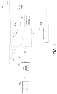
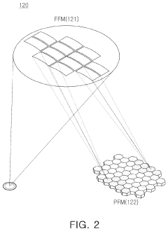
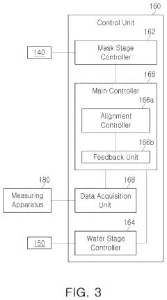
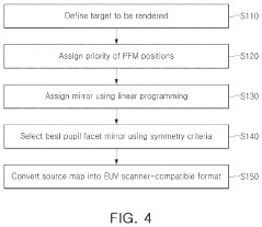
- The implementation of a freeform EUV illumination system using linear programming and priority optimization to assign mirror positions, allowing for the generation of an optimized illumination system that can be converted into a form recognizable by an EUV scanner, thereby improving patterning performance.
Geopolitical Implications for Semiconductor Supply Chain
The geopolitical landscape surrounding EUV lithography has transformed the semiconductor supply chain into a strategic battleground for technological sovereignty. As ASML maintains its monopoly on EUV technology, nations are increasingly viewing semiconductor manufacturing capabilities as critical national security assets. This has led to a complex web of export controls, technology transfer restrictions, and strategic alliances that fundamentally reshape global semiconductor trade patterns.
The United States has implemented comprehensive export controls targeting advanced semiconductor technologies, particularly limiting China's access to EUV lithography equipment. These restrictions extend beyond direct sales to include knowledge transfer, technical support, and component supply chains. Similarly, the Netherlands and Japan have aligned with these policies, creating a coordinated approach to controlling EUV technology proliferation.
In response, China has accelerated its domestic semiconductor initiatives, investing billions in alternative lithography technologies and manufacturing capabilities. This technological decoupling is creating parallel supply chains and standards ecosystems, potentially fragmenting the previously globalized semiconductor industry into geopolitical blocs.
EUV lithography's concentration in specific geographic regions has exposed vulnerabilities in the global semiconductor supply chain. Taiwan's dominant position in advanced chip manufacturing, coupled with ASML's control of EUV technology in the Netherlands, creates critical chokepoints that nations are increasingly seeking to mitigate through reshoring and "friend-shoring" initiatives.
The CHIPS Act in the United States, EU Chips Act in Europe, and similar policies in Japan and South Korea represent unprecedented government interventions in semiconductor manufacturing, directly motivated by concerns over EUV technology access and control. These initiatives are reshaping investment patterns and creating new manufacturing hubs outside traditional centers.
International standards bodies like IEEE and SEMI face mounting pressure as geopolitical tensions influence technical standardization processes. The development of next-generation semiconductor standards increasingly reflects national security considerations alongside technical requirements, with competing standards potentially emerging in different geopolitical spheres.
The concentration of EUV expertise and intellectual property has triggered talent wars between nations, with aggressive recruitment of semiconductor engineers and researchers becoming a dimension of geopolitical competition. This talent migration influences where future innovations in lithography technology will emerge and which nations will control next-generation semiconductor manufacturing capabilities.
International Standards Development and Harmonization
The evolution of Extreme Ultraviolet (EUV) lithography has catalyzed significant changes in international semiconductor standards development. Organizations such as the International Technology Roadmap for Semiconductors (ITRS), now succeeded by the International Roadmap for Devices and Systems (IRDS), have had to adapt their standardization frameworks to accommodate the unique capabilities and requirements of EUV technology.
Global standards bodies including the International Electrotechnical Commission (IEC), Institute of Electrical and Electronics Engineers (IEEE), and SEMI have been working collaboratively to establish harmonized standards for EUV implementation. These efforts focus on ensuring interoperability, safety protocols, and performance metrics that can be universally applied across different manufacturing environments and geographical regions.
The technical complexity of EUV lithography has necessitated unprecedented levels of international cooperation in standards development. Joint technical committees comprising experts from North America, Europe, and Asia have been established to address the multifaceted challenges of integrating EUV technology into existing semiconductor fabrication processes. This collaborative approach has helped bridge differences in regional regulatory frameworks and technical specifications.
Standards harmonization efforts have particularly focused on critical areas such as EUV source specifications, mask infrastructure, resist performance metrics, and defect inspection methodologies. The development of these standards has required balancing the interests of equipment manufacturers, material suppliers, and semiconductor fabrication facilities across different countries.
The World Trade Organization's Technical Barriers to Trade (TBT) Agreement has played a crucial role in facilitating the international adoption of EUV-related standards. By promoting transparency and non-discrimination principles, the TBT framework has helped prevent the emergence of technical regulations that could potentially fragment the global semiconductor market along national or regional lines.
Intellectual property considerations have significantly influenced the standards development process for EUV lithography. Patent pools and licensing frameworks have been established to ensure that essential technologies can be accessed by industry participants worldwide while still providing appropriate compensation to innovators. These mechanisms have been vital in preventing standards from becoming vehicles for market dominance by a small number of technology providers.
The pace of standards development has accelerated to match the rapid advancement of EUV technology. Standards organizations have implemented more agile processes, including the use of preliminary technical reports and living documents that can be updated as the technology matures. This approach has helped maintain the relevance of standards in a rapidly evolving technological landscape.
Unlock deeper insights with Patsnap Eureka Quick Research — get a full tech report to explore trends and direct your research. Try now!
Generate Your Research Report Instantly with AI Agent
Supercharge your innovation with Patsnap Eureka AI Agent Platform!