EUV Lithography: Technological Advancements and Their Applications
OCT 14, 20259 MIN READ
Generate Your Research Report Instantly with AI Agent
Patsnap Eureka helps you evaluate technical feasibility & market potential.
EUV Lithography Evolution and Objectives
Extreme Ultraviolet (EUV) lithography represents a revolutionary advancement in semiconductor manufacturing technology, marking a significant departure from traditional optical lithography methods. The evolution of EUV technology spans several decades, beginning in the 1980s with initial research into short-wavelength lithography techniques. By the 1990s, EUV emerged as a promising candidate for next-generation lithography, utilizing 13.5nm wavelength light to enable the production of increasingly miniaturized semiconductor components.
The development trajectory of EUV lithography has been characterized by persistent technical challenges and breakthrough innovations. Early research focused primarily on fundamental physics and proof-of-concept demonstrations, while the 2000s witnessed intensive efforts to develop practical EUV light sources, specialized optics, and compatible photoresist materials. The 2010s marked a critical transition period as the technology moved from research laboratories to commercial implementation, culminating in ASML's introduction of production-ready EUV lithography systems.
Throughout this evolution, the primary technological objective has remained consistent: enabling the continuation of Moore's Law by facilitating the production of smaller, more densely packed transistors. EUV lithography achieves this through its significantly shorter wavelength compared to previous deep ultraviolet (DUV) systems, allowing for the resolution of features below 10nm with greater precision and fewer processing steps.
Current technological objectives for EUV lithography focus on several key areas: improving system reliability and uptime to meet high-volume manufacturing requirements; increasing throughput to enhance economic viability; reducing defect rates to improve yield; and extending the technology's capabilities to enable future node transitions. Additionally, researchers are exploring complementary technologies such as high-NA (numerical aperture) EUV systems to further extend resolution capabilities.
The industry is also pursuing objectives related to the EUV ecosystem, including the development of more sensitive photoresists, improved mask technologies, and enhanced metrology tools. These supporting technologies are crucial for maximizing the benefits of EUV lithography and ensuring its successful integration into semiconductor manufacturing workflows.
Looking forward, the technological roadmap for EUV lithography aims to support semiconductor scaling through the 3nm node and beyond, potentially enabling feature sizes approaching atomic limits. This continued evolution will require coordinated advancements across multiple disciplines, including optics, materials science, precision engineering, and computational lithography, highlighting the increasingly interdisciplinary nature of semiconductor technology development.
Semiconductor Industry Demand Analysis
The semiconductor industry's demand for advanced lithography technologies, particularly EUV (Extreme Ultraviolet) lithography, has been growing exponentially in recent years. This surge is primarily driven by the continuous miniaturization of semiconductor devices in accordance with Moore's Law, which predicts the doubling of transistor density approximately every two years. As leading semiconductor manufacturers push toward 5nm, 3nm, and even 2nm process nodes, conventional DUV (Deep Ultraviolet) lithography has reached its physical limitations, making EUV technology increasingly indispensable.
Market analysis indicates that the global semiconductor industry, valued at approximately $556 billion in 2021, is projected to reach $1 trillion by 2030, with advanced lithography equipment representing a significant portion of capital expenditure. The demand for EUV lithography systems is particularly strong among leading-edge semiconductor manufacturers, with TSMC, Samsung, and Intel being the primary adopters. These companies are collectively investing billions of dollars in EUV technology to maintain competitive advantages in producing high-performance computing chips, mobile processors, and memory devices.
The COVID-19 pandemic has further accelerated demand for semiconductor devices across various sectors, including data centers, telecommunications, consumer electronics, and automotive industries. This has created a ripple effect, intensifying the need for advanced manufacturing capabilities that only EUV lithography can provide. The global chip shortage that began in 2020 has highlighted the strategic importance of semiconductor manufacturing capacity and technological leadership, prompting governments worldwide to invest in domestic semiconductor ecosystems.
Regional analysis reveals that Asia-Pacific dominates semiconductor manufacturing, with Taiwan and South Korea leading in advanced node production utilizing EUV technology. However, both the United States and European Union have announced significant initiatives to strengthen their semiconductor manufacturing capabilities, including substantial investments in EUV-based fabrication facilities. These geopolitical shifts are expected to diversify the demand for EUV lithography systems geographically over the next decade.
From an application perspective, the demand for EUV lithography is primarily driven by high-volume manufacturing of logic chips for mobile devices, high-performance computing, and artificial intelligence applications. As these sectors continue to grow at double-digit rates annually, the derived demand for EUV technology remains robust. Additionally, emerging applications in quantum computing, autonomous vehicles, and IoT devices are expected to create new demand vectors for advanced semiconductor manufacturing capabilities.
The economic analysis of EUV implementation reveals that despite the high initial capital investment—with each EUV lithography system costing over $150 million—the technology offers compelling long-term cost benefits through simplified manufacturing processes, reduced multi-patterning steps, and improved yields for advanced nodes. This economic rationale further strengthens the business case for EUV adoption across the semiconductor industry.
EUV Technology Status and Barriers
Extreme Ultraviolet (EUV) lithography represents a revolutionary advancement in semiconductor manufacturing, operating at a wavelength of 13.5nm. Currently, the technology has achieved commercial deployment in leading-edge semiconductor fabrication facilities, with ASML maintaining a virtual monopoly as the sole supplier of production-ready EUV lithography systems. Their NXE series machines, particularly the NXE:3400C and newer NXE:3600D models, have been adopted by major semiconductor manufacturers including TSMC, Samsung, and Intel for sub-7nm node production.
Despite significant progress, EUV technology faces several critical barriers. Power source limitations remain a primary challenge, with current EUV light sources struggling to achieve the ideal 250W output power required for optimal wafer throughput. The complex laser-produced plasma system, which generates EUV light by firing CO2 lasers at tin droplets, suffers from conversion efficiency issues, typically achieving only 1-2% efficiency in converting input energy to usable EUV radiation.
Mask defectivity presents another substantial hurdle. Unlike traditional optical lithography, EUV masks cannot use pellicles effectively due to the extreme absorption of EUV wavelengths by most materials. This increases the risk of pattern defects and particulate contamination. Additionally, mask blank production remains challenging with defect rates higher than desired for mass production.
Photoresist performance continues to challenge manufacturers, with current EUV resists facing a difficult trade-off between sensitivity, resolution, and line-edge roughness—the so-called "triangle of death" in resist design. Higher sensitivity resists typically suffer from increased line-edge roughness, compromising pattern fidelity.
Geographically, EUV technology development remains concentrated in specific regions. The Netherlands dominates system development through ASML, while Japan leads in mask and blank production with companies like Lasertec and Hoya. The United States contributes significantly to light source technology through companies like Cymer (now part of ASML), and South Korea and Taiwan have become primary adopters for high-volume manufacturing implementation.
Economic barriers are equally significant, with each EUV lithography system costing approximately $150-200 million, plus substantial facility modification requirements. This restricts adoption to only the largest semiconductor manufacturers and creates a significant entry barrier for smaller players in advanced node production.
Looking forward, stochastic effects at these extremely small dimensions present fundamental physical limitations that will require innovative solutions as the industry pushes toward 3nm nodes and beyond. Random variations in photon absorption and chemical reactions become increasingly problematic as feature sizes approach atomic scales.
Current EUV Implementation Solutions
01 EUV Lithography System Design and Components
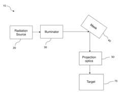
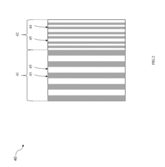
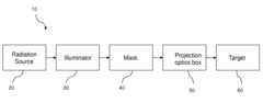
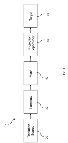
EUV lithography systems incorporate specialized components designed to work with extreme ultraviolet light. These systems typically include radiation sources, illumination optics, reticle stages, projection optics, and wafer stages. The design focuses on maintaining precise alignment and stability while operating in vacuum environments to prevent absorption of EUV radiation by air molecules. Advanced control systems manage thermal effects and vibration to ensure nanometer-level accuracy during the lithographic process.- EUV lithography system components and design: EUV lithography systems incorporate specialized components designed to work with extreme ultraviolet light. These systems typically include radiation sources, optical elements, mirrors, and positioning systems that enable precise pattern transfer at nanometer scales. The design focuses on managing the unique properties of EUV radiation, including its absorption characteristics and interaction with various materials, to achieve high-resolution semiconductor manufacturing.
- Contamination control and mitigation in EUV systems: Contamination control is critical in EUV lithography due to the sensitivity of optical components to even minimal contamination. Various approaches are employed to prevent and mitigate contamination, including specialized cleaning methods, protective layers for optical surfaces, environmental controls, and monitoring systems that detect contamination before it impacts performance. These techniques help maintain the precision and longevity of EUV lithography equipment.
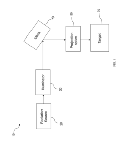
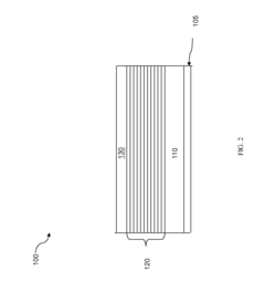
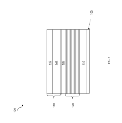
- EUV mask technology and inspection: EUV masks require specialized technology due to the reflective nature of EUV lithography. These masks incorporate multilayer reflective coatings, absorber patterns, and protective features to ensure accurate pattern transfer. Advanced inspection techniques are employed to detect defects, verify pattern accuracy, and ensure mask quality. The development of these masks addresses challenges related to pattern fidelity, defect management, and compatibility with EUV radiation properties.
- Thermal management in EUV lithography: Thermal management is essential in EUV lithography systems due to the high energy levels involved. Various cooling systems, temperature control mechanisms, and thermal isolation techniques are employed to maintain stability and prevent thermal distortion of critical components. These systems help manage heat generated by EUV sources and ensure consistent performance during the lithography process, maintaining the precision required for nanometer-scale manufacturing.
- EUV source technology and optimization: EUV radiation sources represent a critical component of lithography systems, typically utilizing laser-produced plasma or discharge-produced plasma to generate extreme ultraviolet light. These sources must deliver sufficient power while maintaining spectral purity and stability. Various approaches to source design, including optimization of target materials, laser parameters, and collection optics, aim to improve efficiency, reliability, and output power to meet the demanding requirements of high-volume semiconductor manufacturing.
02 EUV Light Sources and Radiation Management
EUV lithography requires specialized light sources that generate radiation at approximately 13.5nm wavelength. These sources typically use laser-produced plasma or discharge-produced plasma technologies where high-energy lasers strike tin droplets or gas to create EUV radiation. The systems incorporate sophisticated collectors, mirrors, and filters to capture, direct, and condition the EUV light. Radiation management includes dose control mechanisms and techniques to minimize stray light while maximizing throughput and uniformity across the exposure field.Expand Specific Solutions03 EUV Masks and Reticle Technology
EUV lithography employs reflective masks rather than the transmissive masks used in conventional lithography. These masks consist of multilayer reflective coatings with patterned absorber layers on their surface. The technology addresses unique challenges including defect mitigation, pattern fidelity, and edge placement accuracy. Advanced inspection and repair techniques ensure mask quality, while pellicle development protects masks from contamination. Reticle handling systems prevent damage and maintain cleanliness in the vacuum environment.Expand Specific Solutions04 EUV Resist Materials and Processing
Specialized photoresist materials are developed for EUV lithography to achieve high resolution with sufficient sensitivity at the 13.5nm wavelength. These materials must balance sensitivity, resolution, line edge roughness, and pattern collapse requirements. The chemistry involves complex interactions between the resist and EUV photons, which have higher energy than conventional UV light. Processing techniques include optimization of post-exposure bake conditions, development processes, and pattern transfer methods to achieve the desired feature dimensions and profiles.Expand Specific Solutions05 Thermal Management and Contamination Control in EUV Systems
EUV lithography systems require sophisticated thermal management to handle heat loads from the high-energy radiation source and maintain dimensional stability of optical components. Cooling systems, temperature sensors, and thermal isolation techniques are employed throughout the system. Additionally, contamination control is critical as even nanometer-scale particles can affect image quality. Systems incorporate vacuum pumps, gas purging mechanisms, and specialized materials to minimize carbon growth, tin debris, and hydrogen-induced effects that could degrade mirrors or contaminate the optical path.Expand Specific Solutions
Leading EUV Equipment Manufacturers and Ecosystem
EUV Lithography technology is currently in a growth phase, with the market expected to reach $10 billion by 2025. The competitive landscape is dominated by a few key players, with ASML (through Carl Zeiss SMT) holding a monopoly on EUV lithography machine production. Leading semiconductor manufacturers like Taiwan Semiconductor Manufacturing Co., Samsung Electronics, and Intel are driving adoption as early implementers. The technology has reached commercial viability but remains highly complex, with companies like TSMC and Samsung pushing boundaries at 5nm and 3nm nodes. Chinese players such as SMIC and Shanghai Micro Electronics Equipment are investing heavily to close the technological gap, while materials suppliers including AGC, Sinyang Semiconductor Materials, and Toppan Holdings provide critical components for the EUV ecosystem.
Taiwan Semiconductor Manufacturing Co., Ltd.
Technical Solution: TSMC has pioneered the implementation of EUV lithography in high-volume manufacturing, beginning with their 7nm+ process node and advancing to 5nm and 3nm nodes. Their EUV implementation strategy involves a multi-layered approach that combines traditional immersion lithography with EUV for critical layers. TSMC's N5 process technology utilizes EUV lithography for up to 14 layers, significantly reducing multi-patterning complexity compared to previous nodes. The company has developed specialized resist materials and mask technologies optimized for their specific EUV implementation, achieving line widths below 30nm with high yield rates. TSMC has also invested in custom computational lithography techniques to enhance EUV pattern fidelity and resolution, including optical proximity correction algorithms specifically tailored for EUV wavelengths. Their EUV integration includes advanced metrology systems for defect inspection and process control, ensuring consistent quality across wafers.
Strengths: Industry-leading implementation of EUV at scale with proven high-volume manufacturing capability; superior yield management; extensive experience across multiple process nodes. Weaknesses: High capital expenditure requirements; dependency on ASML as the sole EUV equipment supplier; challenges in maintaining sufficient EUV power sources for expanding production capacity.
Intel Corp.
Technical Solution: Intel has developed a comprehensive EUV lithography implementation strategy for their process technology roadmap, particularly for their Intel 4 (previously 7nm) and beyond nodes. Their approach includes specialized resist chemistry optimized for EUV sensitivity and line edge roughness control. Intel's EUV technology incorporates advanced computational lithography techniques, including source mask optimization and inverse lithography technology, to maximize pattern fidelity. The company has invested in developing custom pellicles to protect EUV masks from contamination while minimizing transmission loss. Intel's EUV implementation includes specialized metrology solutions for detecting sub-resolution defects and ensuring pattern accuracy. Their EUV strategy also encompasses innovations in mask infrastructure, including advanced absorber materials and phase-shifting techniques to enhance contrast. Intel has reported achieving critical dimensions below 25nm using their EUV process, with plans to extend EUV usage to more layers in future nodes.
Strengths: Extensive R&D capabilities with significant intellectual property in EUV implementation; vertical integration allowing for customized solutions; strong computational lithography expertise. Weaknesses: Delayed implementation compared to competitors; challenges in scaling EUV implementation to high-volume manufacturing; historical difficulties in process node transitions.
Critical EUV Patents and Technical Innovations
Extreme Ultraviolet Lithography Process and Mask
PatentActiveUS20150168845A1
Innovation
- The implementation of a nearly on-axis illumination with partial coherence less than 0.3 in an EUV lithography system, combined with an EUV mask featuring a first region with main polygons and a second region with sub-resolution polygons, and a spatial filter to remove most non-diffracted light, enhancing spatial frequency resolution and uniformity of exposure intensity.
Extreme Ultraviolet Lithography Process And Mask
PatentActiveUS20150085268A1
Innovation
- A mask structure incorporating a reflective multilayer with a flare-suppressing absorption stack (FSAS) and a flare-suppressing-by-phase-shifting (FSbPhS) layer is used to absorb and destructively interfere OOB radiation, specifically DUV flare, enhancing reflectivity and minimizing EUV light absorption.
Supply Chain Resilience for EUV Technology
The EUV lithography supply chain represents one of the most complex and vulnerable technological ecosystems in the semiconductor industry. The highly specialized nature of EUV technology creates significant dependencies on a limited number of suppliers, with ASML holding a virtual monopoly on EUV lithography systems. This concentration of critical capabilities introduces substantial risks to the global semiconductor manufacturing infrastructure.
Supply chain disruptions affecting EUV technology can emerge from various sources, including geopolitical tensions, trade restrictions, natural disasters, and public health crises. The COVID-19 pandemic demonstrated how quickly global supply chains can be compromised, with semiconductor manufacturers experiencing delays in equipment delivery and installation. For EUV lithography specifically, these disruptions are magnified by the technology's reliance on rare materials and highly specialized components.
Building resilience into the EUV supply chain requires multi-faceted approaches. Diversification of supplier networks represents a critical strategy, though challenging given the specialized expertise required. Leading semiconductor manufacturers have begun establishing strategic partnerships with key suppliers, implementing dual-sourcing strategies where possible, and developing contingency plans for critical components. Geographic diversification of manufacturing facilities also helps mitigate regional disruption risks.
Inventory management strategies have evolved significantly, with many companies moving beyond just-in-time models toward maintaining strategic reserves of critical EUV components. This approach, while capital-intensive, provides a buffer against short-term supply disruptions. Advanced analytics and AI-driven supply chain monitoring systems enable early detection of potential disruptions, allowing for proactive mitigation measures.
The development of domestic capabilities in EUV technology has become a strategic priority for many nations. Government initiatives in the United States, European Union, Japan, and South Korea have allocated significant funding to strengthen local semiconductor ecosystems, including EUV supply chains. These efforts aim to reduce dependency on single geographic regions and create more resilient supply networks.
Technological innovation itself contributes to supply chain resilience. Research into alternative materials, simplified designs, and more standardized components could reduce dependencies on specific suppliers. Additionally, advances in digital twins and simulation technologies allow companies to virtually test supply chain scenarios and optimize contingency planning before disruptions occur.
Environmental Impact of EUV Manufacturing Processes
The manufacturing processes involved in EUV lithography present significant environmental challenges that warrant careful consideration. The production of EUV systems requires substantial energy consumption, with a single EUV lithography machine consuming approximately 1 megawatt of power during operation. This high energy demand contributes to increased carbon emissions, particularly in regions where electricity generation relies heavily on fossil fuels.
Water usage represents another critical environmental concern. The manufacturing and operation of EUV systems require ultra-pure water in substantial quantities—estimates suggest that a semiconductor fabrication facility using EUV technology may consume between 2-5 million gallons of water daily. This places considerable strain on local water resources, especially in water-stressed regions where semiconductor manufacturing clusters are often located.
Chemical waste management poses additional environmental challenges. The EUV process utilizes various chemicals including photoresists, developers, and cleaning agents that contain potentially hazardous compounds. These substances require specialized disposal procedures to prevent soil and groundwater contamination. Industry data indicates that a typical semiconductor facility may generate several tons of chemical waste monthly, necessitating robust waste management protocols.
The production of EUV components also involves rare earth elements and specialized materials with environmentally intensive extraction processes. Mining operations for these materials can lead to habitat destruction, soil erosion, and water pollution in source regions. The global supply chain for these materials creates a distributed environmental footprint across multiple countries and ecosystems.
Recent industry initiatives have begun addressing these environmental concerns. Leading manufacturers have implemented closed-loop water recycling systems that can reduce freshwater consumption by up to 60%. Energy efficiency improvements in newer generation EUV systems have achieved approximately 15-20% reduction in power requirements compared to earlier models. Additionally, chemical substitution programs have successfully replaced several highly toxic compounds with more environmentally benign alternatives.
Regulatory frameworks are evolving to address the environmental impact of semiconductor manufacturing. The European Union's Restriction of Hazardous Substances (RoHS) directive and similar regulations in other regions have prompted manufacturers to develop compliance strategies that minimize environmental harm while maintaining technological advancement. Industry consortia have established voluntary environmental performance standards that exceed regulatory requirements, demonstrating a growing commitment to sustainable manufacturing practices.
Unlock deeper insights with Patsnap Eureka Quick Research — get a full tech report to explore trends and direct your research. Try now!
Generate Your Research Report Instantly with AI Agent
Supercharge your innovation with Patsnap Eureka AI Agent Platform!