Examining OLED vs MicroLED Materials for Durability
OCT 24, 20259 MIN READ
Generate Your Research Report Instantly with AI Agent
Patsnap Eureka helps you evaluate technical feasibility & market potential.
OLED and MicroLED Evolution and Objectives
Display technology has undergone significant evolution over the past decades, with OLED (Organic Light-Emitting Diode) emerging as a revolutionary advancement in the early 2000s. This technology marked a departure from traditional LCD displays by eliminating the need for backlighting, allowing for thinner, more flexible screens with superior contrast ratios and energy efficiency. The development of OLED technology can be traced back to Eastman Kodak's pioneering work in 1987, which laid the foundation for commercial applications that began to materialize in the early 2000s.
MicroLED represents the next frontier in display technology, with its development gaining momentum since the mid-2010s. Unlike OLED, which uses organic compounds, MicroLED utilizes inorganic gallium nitride-based materials to create self-emissive pixels at a microscopic scale. This fundamental material difference has profound implications for durability, which stands as a central focus in the technological competition between these two display technologies.
The evolution of both technologies has been driven by increasing demands for higher resolution, improved energy efficiency, and enhanced durability in consumer electronics, automotive displays, and professional visualization systems. OLED has established market dominance in premium smartphones and high-end televisions, while MicroLED is positioning itself as the potential successor due to its promising durability characteristics.
The primary objective in examining OLED versus MicroLED materials for durability is to comprehensively understand the inherent limitations of organic materials in OLED displays compared to the inorganic compounds in MicroLED. OLED displays face challenges related to organic material degradation, particularly blue OLED compounds which typically have shorter lifespans than red and green counterparts. This degradation manifests as color shift and reduced brightness over time, especially under high-brightness operating conditions.
MicroLED technology aims to overcome these durability constraints through its use of inorganic materials that demonstrate superior resistance to degradation. The objective is to quantify this advantage and determine whether MicroLED can deliver the theoretical 100,000+ hour lifespan without significant brightness deterioration or color shift that would represent a substantial improvement over current OLED capabilities.
Additionally, this technical examination seeks to establish clear metrics for comparing durability across different usage scenarios, including high-brightness environments, variable temperature conditions, and continuous operation requirements. Understanding these parameters is crucial for determining the appropriate technology for specific applications ranging from consumer devices to automotive displays and commercial signage where operational longevity is paramount.
Market Demand Analysis for Durable Display Technologies
The display technology market is witnessing a significant shift toward more durable solutions, driven primarily by consumer demand for longer-lasting devices and industrial requirements for reliable performance in harsh environments. Current market research indicates that the global display market is expected to reach $177 billion by 2026, with durability becoming a key differentiator among competing technologies.
Consumer electronics represent the largest segment demanding durable display technologies, with smartphones and wearables leading the charge. Smartphone manufacturers report that display damage accounts for approximately 30% of warranty claims, creating substantial financial incentives to adopt more durable display solutions. The wearable technology sector, growing at 15% annually, particularly demands displays that can withstand constant exposure, physical impact, and various environmental conditions.
Automotive displays constitute another rapidly expanding market segment, projected to grow at 17% annually through 2028. These applications require displays capable of withstanding extreme temperature variations, vibration, and prolonged UV exposure. The emerging trend of larger dashboard displays and entertainment systems in vehicles has intensified the need for materials that maintain visual performance while offering exceptional durability.
Commercial and industrial sectors are increasingly adopting digital signage and interactive displays, with durability requirements often exceeding those of consumer applications. These installations frequently operate continuously in public spaces, requiring resistance to vandalism, weather exposure, and minimal degradation over extended periods. The industrial display market segment values longevity over cutting-edge visual performance, creating distinct requirements compared to consumer markets.
Healthcare represents a specialized but growing market for durable displays, with requirements for chemical resistance, sterilization capability, and consistent performance in critical applications. Medical display devices must maintain precise color accuracy and resolution while withstanding frequent cleaning with harsh disinfectants.
Market analysis reveals a growing premium segment willing to pay 20-40% more for displays with proven durability advantages. This trend is particularly evident in luxury consumer electronics and professional equipment markets. Manufacturers capable of demonstrating superior durability metrics through standardized testing are capturing increased market share despite higher initial pricing.
Regional market variations show that durability requirements differ significantly across global markets. Emerging economies often prioritize repairability and longevity over cutting-edge features, while developed markets segment into premium durability-focused consumers and price-sensitive segments willing to accept shorter replacement cycles.
Current Durability Challenges in Display Materials
Both OLED and MicroLED display technologies face significant durability challenges that impact their performance, lifespan, and market adoption. OLED displays suffer from organic material degradation, with blue OLED compounds particularly susceptible to shorter lifespans compared to red and green counterparts. This differential aging leads to color shift over time, compromising display quality. Additionally, OLED materials are highly sensitive to moisture and oxygen exposure, necessitating complex encapsulation techniques that add to manufacturing complexity and cost.
Burn-in remains a persistent issue for OLED displays, where static image elements cause uneven pixel degradation, resulting in ghost images that permanently affect screen quality. This problem is particularly pronounced in applications displaying static interface elements for extended periods, such as navigation systems or status indicators in automotive displays.
MicroLED technology, while promising superior theoretical durability, faces its own set of challenges. The inorganic LED materials, though more inherently stable than organic compounds, encounter issues at the microscopic scale required for high-resolution displays. Quantum efficiency droop—where LED efficiency decreases at higher current densities—becomes more pronounced at the micro scale, affecting brightness consistency and power efficiency.
Heat management presents a critical challenge for both technologies but manifests differently. OLED materials degrade faster at elevated temperatures, while MicroLED displays generate significant heat during operation that must be effectively dissipated to prevent accelerated aging and performance degradation. This thermal management becomes increasingly complex as pixel densities increase and device form factors become thinner.
Manufacturing-related durability issues also differ between technologies. MicroLED displays face challenges with mechanical stability during the mass transfer process, where millions of tiny LED chips must be precisely placed. Defects in this process can lead to dead pixels and reduced yield rates. Meanwhile, OLED manufacturing struggles with consistent thin-film deposition across large areas, leading to potential weak points in the display structure.
Environmental factors affect both technologies differently. OLED displays are particularly vulnerable to ultraviolet light exposure, which accelerates the breakdown of organic materials. MicroLED materials show better resistance to UV radiation but may experience issues with coefficient of thermal expansion mismatches between different material layers, potentially leading to mechanical stress and failure points during temperature fluctuations.
These durability challenges directly impact product lifespans, warranty considerations, and ultimately consumer confidence, making them critical factors in the competitive landscape between these emerging display technologies.
Current Material Solutions for Display Durability
01 Encapsulation techniques for OLED and MicroLED durability
Various encapsulation methods are employed to protect OLED and MicroLED materials from environmental factors that cause degradation. These techniques include thin-film encapsulation, hermetic sealing, and multi-layer barrier structures that prevent moisture and oxygen penetration. Advanced encapsulation technologies significantly extend the operational lifetime of these display technologies by creating effective barriers against environmental contaminants that would otherwise lead to pixel degradation and device failure.- Encapsulation techniques for OLED and MicroLED protection: Various encapsulation methods are employed to protect OLED and MicroLED materials from environmental factors that degrade durability. These include thin-film encapsulation layers, hermetic sealing technologies, and multi-layer barrier structures that prevent moisture and oxygen penetration. Advanced encapsulation techniques significantly extend the operational lifetime of these display technologies by creating effective barriers against environmental degradation factors.
- Material composition improvements for enhanced stability: Research focuses on developing more stable organic and inorganic materials for OLED and MicroLED applications. This includes modified emitter compounds with improved thermal stability, novel host materials that resist degradation, and more robust charge transport layers. These material innovations address common failure mechanisms such as thermal decomposition, photo-oxidation, and molecular reorganization that typically limit device longevity.
- Thermal management solutions for extended lifetime: Effective thermal management strategies are crucial for maintaining OLED and MicroLED durability. Approaches include integration of heat dissipation structures, thermally conductive substrates, and advanced thermal interface materials. These solutions prevent temperature-induced degradation mechanisms by efficiently removing heat from active device regions, thereby extending operational lifetime and maintaining consistent performance characteristics over time.
- Interface engineering to reduce degradation mechanisms: Interface engineering between different functional layers in OLED and MicroLED devices significantly impacts durability. Techniques include gradient composition interfaces, buffer layers to prevent ion migration, and surface treatments to improve adhesion and reduce interfacial defects. These approaches minimize charge accumulation at interfaces and prevent delamination issues that commonly lead to device failure over time.
- Drive scheme optimization for uniform aging: Advanced driving methods and compensation algorithms are developed to ensure uniform aging of OLED and MicroLED materials. These include pixel compensation circuits, current distribution optimization, and adaptive brightness control systems that account for differential aging rates. By managing electrical stress more effectively across the display, these techniques prevent localized degradation and maintain consistent brightness and color reproduction throughout the device lifetime.
02 Material composition innovations for enhanced stability
Novel material compositions are being developed to inherently improve the durability of OLED and MicroLED displays. These include modified emissive materials with enhanced thermal stability, more robust charge transport layers, and alternative electrode materials that resist oxidation. By engineering materials at the molecular level, researchers have created compounds that maintain their electroluminescent properties longer under operational conditions, resulting in displays with extended lifespans and reduced color shift over time.Expand Specific Solutions03 Thermal management solutions for longevity
Effective thermal management is critical for extending the durability of OLED and MicroLED displays. Innovations include heat-dissipating substrates, thermal interface materials, and active cooling systems that prevent temperature-induced degradation. These solutions help maintain optimal operating temperatures, preventing accelerated aging of organic materials in OLEDs and junction degradation in MicroLEDs, thereby significantly extending device lifetime and maintaining brightness uniformity across the display.Expand Specific Solutions04 Structural design improvements for mechanical durability
Structural enhancements in OLED and MicroLED displays focus on improving mechanical durability against physical stresses. These include flexible substrates, stress-relief layers, and novel pixel architectures that can withstand bending, folding, and impact. Advanced lamination techniques and protective overlays provide additional mechanical protection while maintaining optical performance. These structural innovations enable displays that can endure physical handling and environmental stresses without compromising their functional integrity.Expand Specific Solutions05 Driving method optimizations for extended lifetime
Specialized driving methods and compensation algorithms are being implemented to extend the operational lifetime of OLED and MicroLED displays. These include current-programmed pixel circuits, aging compensation algorithms, and adaptive brightness control systems that reduce stress on emissive materials. By intelligently managing how pixels are driven based on content and usage patterns, these methods minimize degradation mechanisms like current-induced heating and uneven aging, resulting in displays that maintain consistent performance characteristics over extended periods.Expand Specific Solutions
Key Industry Players in Advanced Display Technologies
The OLED vs MicroLED materials durability landscape is currently in a transitional phase, with OLED technology dominating the commercial market while MicroLED emerges as a promising alternative. The global display market is projected to reach $200 billion by 2025, with durability being a critical differentiator. OLED technology, led by Samsung Electronics, LG Display, and BOE Technology, has achieved commercial maturity but faces challenges with organic material degradation. MicroLED technology, being developed by companies like X Display Co., Applied Materials, and Samsung, offers superior durability with inorganic materials that resist burn-in and provide longer lifespans. This technological competition is driving significant R&D investment across both technologies, with major players pursuing parallel development strategies to secure market position.
BOE Technology Group Co., Ltd.
Technical Solution: BOE has developed comprehensive material solutions for both OLED and MicroLED durability challenges. For OLED technology, BOE employs a proprietary multi-stack emission layer structure that distributes electrical and thermal stress across multiple organic compounds, extending operational lifetime by up to 40% compared to conventional single-stack designs. Their OLED panels feature advanced thin-film encapsulation technology with alternating inorganic (SiNx) and organic layers that achieve water vapor transmission rates below 10^-6 g/m²/day, providing robust protection against moisture-induced degradation. BOE has also pioneered self-compensating pixel circuits that adjust current flow based on real-time monitoring of OLED degradation, maintaining consistent brightness levels throughout the panel's lifespan. For MicroLED development, BOE utilizes GaN-on-Silicon technology with proprietary buffer layers that reduce lattice mismatch and defect density, resulting in LEDs with improved electrical efficiency and thermal stability. Their MicroLED manufacturing process incorporates a novel mass transfer technique with placement accuracy exceeding 99.99%, crucial for maintaining display integrity over extended use periods. BOE's latest MicroLED materials demonstrate exceptional resistance to environmental stressors, with accelerated aging tests showing minimal degradation after exposure to temperature cycling between -40°C and 85°C.
Strengths: BOE's vertical integration across the display supply chain enables tight quality control and material optimization. Their OLED encapsulation technology demonstrates industry-leading barrier properties against environmental contaminants. Their MicroLED development benefits from extensive manufacturing infrastructure and expertise in semiconductor processing. Weaknesses: BOE's OLED technology still faces challenges with blue pixel degradation, requiring complex compensation algorithms to maintain color accuracy over time. Their MicroLED manufacturing yields remain relatively low compared to conventional display technologies, contributing to high production costs.
Samsung Electronics Co., Ltd.
Technical Solution: Samsung has developed a comprehensive approach to OLED and MicroLED durability through advanced material science. For OLEDs, Samsung employs proprietary blue phosphorescent materials that extend operational lifetime by up to 30% compared to conventional fluorescent compounds. Their OLED panels incorporate multi-layer thin film encapsulation (TFE) technology with alternating inorganic and organic layers that significantly reduce moisture penetration, addressing one of OLED's primary durability challenges. For MicroLED, Samsung has pioneered GaN-based RGB MicroLED technology with direct RGB color emission that eliminates the need for color conversion layers, reducing heat generation and extending panel lifespan. Their MicroLED displays utilize a proprietary transfer process that maintains 99.999% placement accuracy, crucial for long-term display stability. Samsung's latest MicroLED materials demonstrate remarkable resistance to image retention, with burn-in tests showing negligible degradation after 10,000 hours of operation, approximately 3-4 times better than their premium OLED panels.
Strengths: Samsung's vertical integration allows for complete control over material development and manufacturing processes, resulting in industry-leading durability metrics. Their MicroLED technology demonstrates superior brightness stability (maintaining over 95% brightness after 100,000 hours) and exceptional resistance to environmental factors. Weaknesses: Samsung's MicroLED manufacturing remains extremely costly with low yields, limiting mass market adoption. Their OLED materials, while improved, still suffer from inherent blue pixel degradation issues that affect long-term color accuracy.
Critical Patents and Innovations in Display Material Science
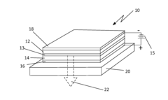
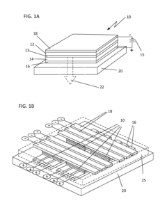
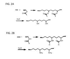
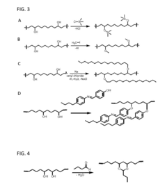
Organic light emitting diodes
PatentInactiveUS20160181570A1
Innovation
- A dual-acting coating material based on a copolymer of ethylene and substituted vinyl is applied to OLEDs, incorporating hydrophobic substituents to create a barrier against oxygen and water permeation, using techniques such as functionalizing vinyl alcohol or vinyl amine segments with water-repellent groups or cross-linking agents to enhance barrier properties.
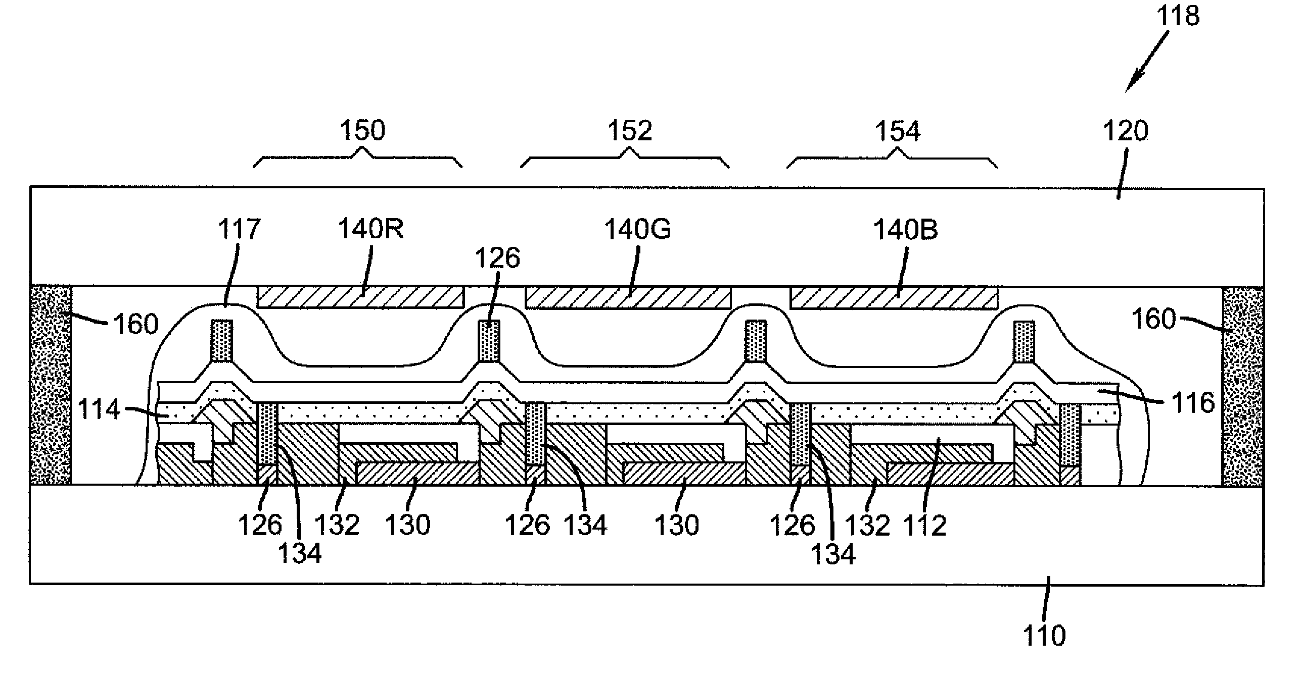
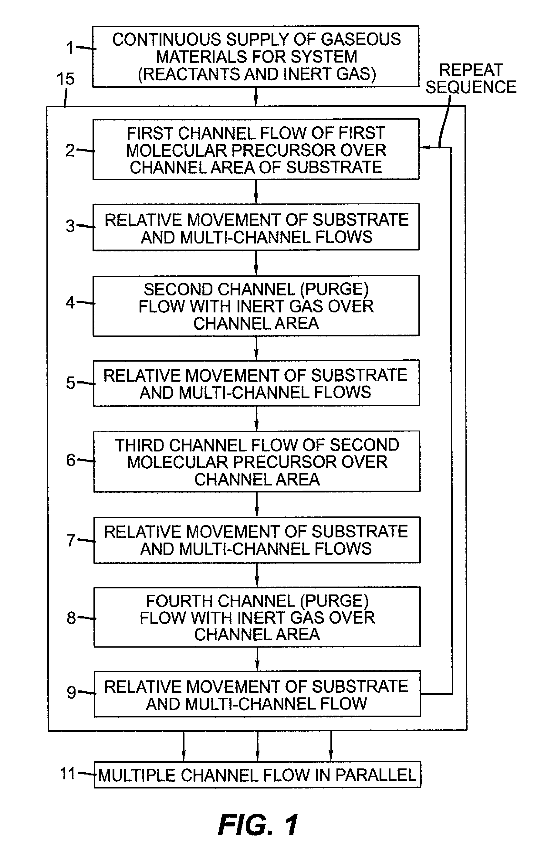
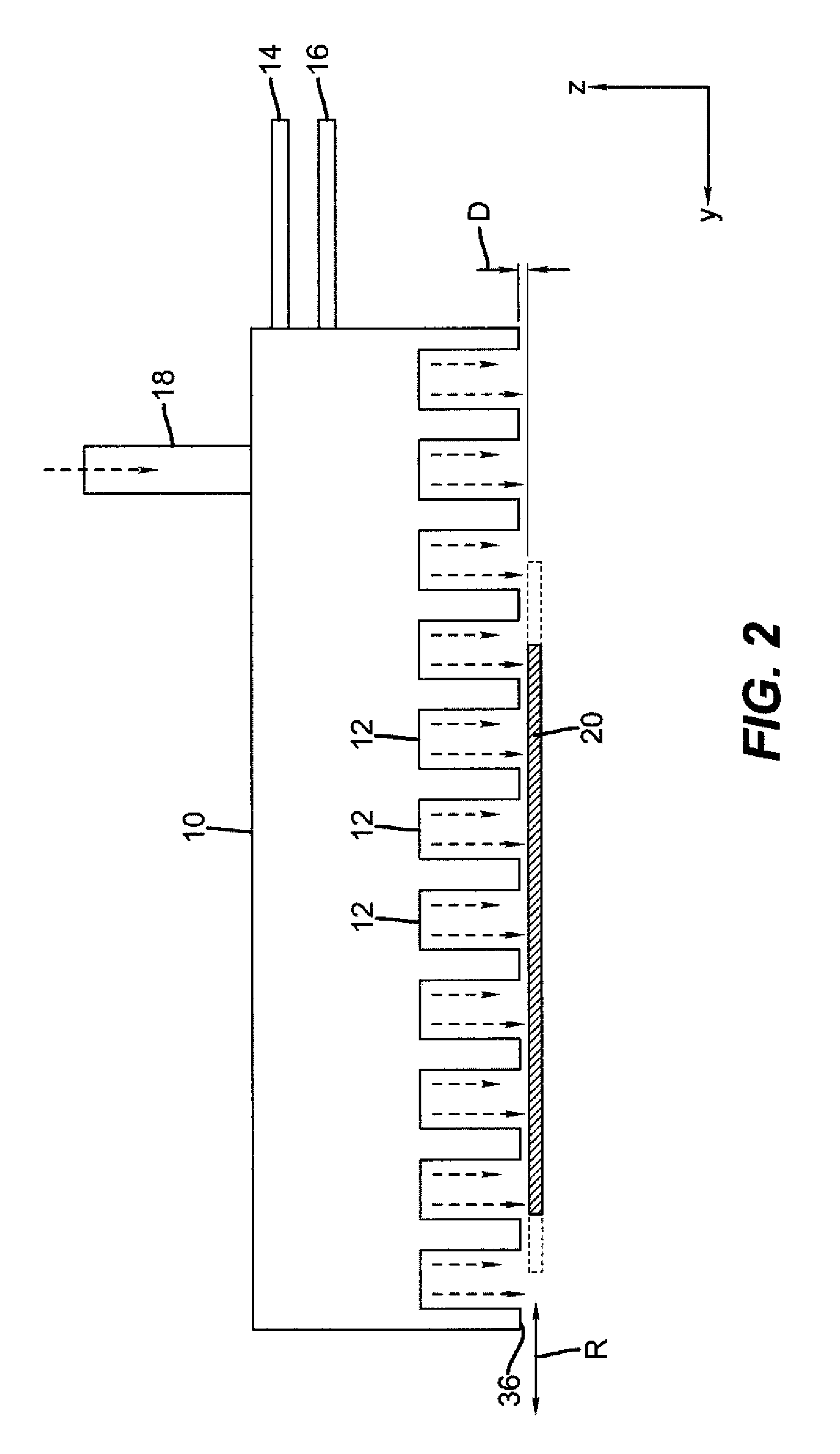
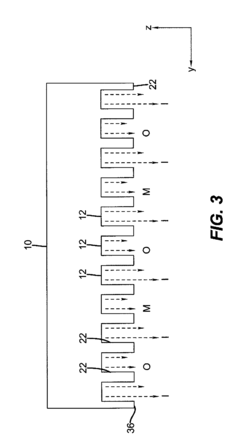
Process for forming thin film encapsulation layers
PatentActiveUS20120070942A1
Innovation
- A spatially dependent ALD process is employed, where a series of gas flows including a reactive metal precursor, inert purge gas, and a second reactive gas are directed along parallel elongated output openings, allowing for continuous substrate movement and operation at or above atmospheric pressure, enabling the deposition of metal-oxide thin films without the need for vacuum processing.
Environmental Impact and Sustainability Considerations
The environmental footprint of display technologies has become increasingly important as consumer electronics proliferate globally. When comparing OLED and MicroLED materials from a sustainability perspective, several critical factors emerge that influence their overall environmental impact throughout their lifecycle.
OLED displays utilize organic compounds that require fewer raw materials in production compared to traditional LCD technologies. However, these organic materials often contain rare elements like iridium, which presents sustainability challenges due to limited global supplies and environmentally problematic extraction processes. Additionally, the manufacturing of OLED panels typically involves energy-intensive vacuum deposition processes and requires various solvents that may contribute to environmental pollution if not properly managed.
MicroLED technology, while still emerging, presents a different environmental profile. The production of MicroLEDs relies heavily on gallium nitride and other semiconductor materials that require significant energy input during manufacturing. However, the exceptional durability of MicroLED materials potentially offsets these initial environmental costs through extended product lifespans, reducing electronic waste generation over time.
Energy efficiency during operation represents another crucial sustainability factor. OLEDs consume minimal power when displaying dark content due to their emissive nature, but their overall efficiency degrades over time. MicroLEDs demonstrate superior energy efficiency across their operational lifespan, potentially resulting in lower lifetime carbon emissions despite higher initial manufacturing energy requirements.
End-of-life considerations reveal further distinctions between these technologies. OLED panels present recycling challenges due to their multi-layer organic structure and the presence of various metals and adhesives. MicroLED displays, while also complex, contain more recoverable inorganic materials that may be more amenable to established recycling processes, though specialized techniques are still under development.
Water usage represents another environmental concern, with both technologies requiring ultra-pure water during manufacturing. OLED production typically demands more extensive cleaning processes due to sensitivity to contaminants, while MicroLED fabrication requires substantial water resources for semiconductor processing and cooling systems.
Hazardous material content also differs between the technologies. OLEDs often contain potentially harmful substances in their organic layers, while MicroLEDs generally incorporate fewer toxic materials but rely on semiconductor processing chemicals that require careful handling and disposal.
As sustainability becomes increasingly central to consumer and corporate decision-making, manufacturers of both technologies are investing in cleaner production methods, improved material efficiency, and enhanced recyclability to reduce their environmental footprint while maintaining performance advantages.
Manufacturing Scalability and Cost Analysis
The manufacturing scalability of OLED and MicroLED technologies presents significant contrasts that directly impact their market adoption and cost structures. OLED manufacturing has matured considerably over the past decade, with established production lines utilizing vacuum thermal evaporation for small molecules and solution processing for polymers. These processes have achieved economies of scale, particularly for smartphone displays, resulting in production costs decreasing by approximately 35% between 2015 and 2022.
In contrast, MicroLED manufacturing remains in its nascent stages with substantial scalability challenges. The primary bottleneck lies in the mass transfer process, where millions of microscopic LED chips must be precisely positioned onto display substrates. Current techniques include laser transfer, electrostatic transfer, and mechanical pick-and-place methods, each with varying yields and throughput limitations. Industry data indicates that mass transfer yields below 99.999% render large-scale MicroLED production economically unviable.
Cost analysis reveals that OLED production currently benefits from amortized equipment investments and optimized supply chains. The average manufacturing cost for OLED displays ranges from $40-100 per square foot depending on specifications, with material costs constituting approximately 70% of total production expenses. Organic materials procurement remains a significant cost factor, though prices have stabilized as more suppliers have entered the market.
MicroLED manufacturing costs are substantially higher, estimated at 8-12 times that of comparable OLED displays in 2023. This disparity stems from low yields, specialized equipment requirements, and limited production volumes. The cost structure breakdown shows that 45% of expenses derive from the mass transfer process alone, while materials account for only 25% of total costs—a ratio expected to shift as manufacturing techniques mature.
Equipment investment presents another critical dimension of manufacturing economics. OLED production lines typically require $50-200 million in capital expenditure depending on capacity, whereas MicroLED facilities demand $200-500 million for comparable output volumes, with significantly higher costs per unit produced during initial scaling phases.
Future projections suggest MicroLED manufacturing costs could decrease by 60-70% over the next five years as mass transfer technologies improve and production volumes increase. However, achieving cost parity with OLED remains unlikely before 2028-2030, particularly for smaller display applications where OLED manufacturing efficiency continues to improve through iterative optimization.
Unlock deeper insights with Patsnap Eureka Quick Research — get a full tech report to explore trends and direct your research. Try now!
Generate Your Research Report Instantly with AI Agent
Supercharge your innovation with Patsnap Eureka AI Agent Platform!