How Do SiC MOSFETs Compare To Next-Generation Power Devices?
SEP 8, 20259 MIN READ
Generate Your Research Report Instantly with AI Agent
Patsnap Eureka helps you evaluate technical feasibility & market potential.
SiC MOSFET Evolution and Performance Objectives
Silicon Carbide (SiC) MOSFETs have emerged as revolutionary components in power electronics, marking a significant departure from traditional silicon-based devices. The evolution of SiC technology began in the early 1990s with rudimentary research devices, progressing through several generations of refinement to today's commercially viable products. This technological journey has been driven by increasing demands for higher efficiency, greater power density, and operation in extreme environments that silicon devices simply cannot address.
The first commercial SiC MOSFETs, introduced around 2011, offered switching speeds and thermal capabilities that outperformed silicon counterparts but suffered from reliability issues and high production costs. Second-generation devices (2014-2017) featured improved channel mobility and reduced on-resistance, while third-generation products (2018-present) have achieved significant cost reductions and enhanced ruggedness, making them viable for mainstream applications.
Current performance objectives for SiC MOSFETs focus on several critical parameters. Reducing specific on-resistance (RDS(on)) remains a primary goal, with industry targets aiming for values below 1.5 mΩ·cm² for 1200V devices. This represents a fundamental advantage over silicon, where theoretical limits prevent achieving comparable performance at high voltage ratings.
Switching performance optimization constitutes another key objective, with efforts directed toward minimizing gate charge and reducing parasitic capacitances to enable higher frequency operation while maintaining switching losses below 10% of silicon IGBTs at equivalent ratings. Temperature performance targets include stable operation at junction temperatures exceeding 200°C, significantly beyond silicon's practical limit of approximately 150°C.
Reliability enhancement represents perhaps the most crucial evolutionary goal, addressing historical concerns about gate oxide integrity and threshold voltage stability. Current objectives include achieving device lifetimes exceeding 20 years under typical operating conditions, with minimal parametric drift throughout the operational lifetime.
Cost reduction trajectories aim to narrow the price premium over silicon alternatives from the historical 3-5x to below 1.5x through manufacturing scale improvements and yield enhancements. This economic evolution is essential for broader market adoption beyond premium applications where performance advantages already justify the cost differential.
Looking forward, the SiC MOSFET roadmap includes development of higher voltage ratings (3.3kV-10kV) for grid applications, further refinement of packaging technologies to maximize thermal performance, and continued advancement in wafer quality to reduce defect densities below 1 per cm².
Market Demand Analysis for Wide Bandgap Power Devices
The wide bandgap (WBG) power device market is experiencing unprecedented growth, driven by increasing demand for energy-efficient power conversion systems across multiple industries. The global WBG semiconductor market, valued at approximately $1.3 billion in 2022, is projected to reach $6.5 billion by 2030, representing a compound annual growth rate (CAGR) of over 25%. Silicon carbide (SiC) devices currently dominate this market segment, accounting for roughly 63% of the total WBG market share, with gallium nitride (GaN) comprising most of the remainder.
Electric vehicle (EV) applications represent the largest and fastest-growing market segment for WBG power devices. As global EV sales continue to surge—reaching 10.5 million units in 2022 and expected to exceed 30 million by 2030—demand for SiC MOSFETs in particular has intensified. These devices enable higher-efficiency power conversion, faster charging capabilities, and extended vehicle range through reduced power losses in inverters and onboard chargers.
Industrial power conversion represents another significant market driver, with WBG devices increasingly deployed in motor drives, uninterruptible power supplies, and industrial automation systems. The industrial sector's push toward higher energy efficiency standards and smaller form factors has accelerated adoption, with the industrial WBG market segment growing at approximately 22% annually.
Renewable energy systems constitute a third major market segment, with solar inverters and wind power converters benefiting from the superior switching characteristics and thermal performance of WBG devices. The global solar PV capacity additions reached 239 GW in 2022, creating substantial demand for high-efficiency power conversion solutions. SiC devices in particular have demonstrated the ability to increase solar inverter efficiency by up to 2 percentage points compared to silicon-based alternatives.
Consumer electronics and telecommunications infrastructure represent emerging application areas with significant growth potential. The deployment of 5G networks has created demand for more efficient power amplifiers and base station power supplies, where GaN devices offer particular advantages due to their high-frequency performance characteristics.
Regional analysis reveals that Asia-Pacific currently leads WBG device consumption, accounting for approximately 45% of global demand, followed by North America (28%) and Europe (22%). China's aggressive electric vehicle and renewable energy initiatives have positioned it as the single largest market for WBG power semiconductors.
Despite strong market demand, several factors constrain wider adoption, including higher device costs compared to silicon alternatives, supply chain constraints, and reliability concerns in certain applications. However, as manufacturing scales increase and technology matures, the cost differential is narrowing, with SiC device prices declining by approximately 10-15% annually.
Current Technological Limitations of SiC MOSFETs
Despite the significant advancements in SiC MOSFET technology, several technological limitations continue to challenge their widespread adoption and optimal performance. The most prominent issue remains the relatively high defect density in SiC substrates compared to traditional silicon. These defects, including micropipes, dislocations, and basal plane defects, can significantly impact device reliability and performance, particularly under high-stress operating conditions.
Channel mobility represents another critical limitation. SiC MOSFETs typically exhibit channel mobility values that are substantially lower than theoretical predictions, primarily due to interface traps at the SiC/SiO2 boundary. This reduced mobility directly impacts the device's on-resistance, limiting efficiency gains in high-current applications and necessitating larger die sizes to achieve desired current ratings.
The gate oxide reliability in SiC MOSFETs presents ongoing challenges. The higher electric field strength in SiC devices places increased stress on the gate oxide layer, potentially leading to premature oxide breakdown or threshold voltage instability. This becomes particularly problematic in applications requiring long-term reliability under extreme conditions.
Manufacturing costs continue to be a significant barrier to wider adoption. While production volumes have increased and costs have decreased, SiC wafers remain substantially more expensive than silicon alternatives. The complex manufacturing processes, including high-temperature annealing steps and specialized epitaxial growth techniques, contribute to higher production costs that are ultimately reflected in device pricing.
Thermal management presents unique challenges for SiC MOSFETs. Although these devices can operate at higher temperatures than silicon counterparts, this capability often requires advanced packaging solutions capable of handling increased thermal loads. The thermal conductivity of SiC, while superior to silicon, still necessitates careful thermal design considerations, particularly in high-power density applications.
Switching performance limitations also exist, particularly regarding parasitic capacitances and inductances. While SiC MOSFETs offer faster switching capabilities than silicon devices, they remain susceptible to ringing and electromagnetic interference issues that can limit practical switching frequencies in real-world applications.
The body diode performance in SiC MOSFETs exhibits higher forward voltage drop and slower reverse recovery characteristics compared to discrete SiC Schottky diodes. This limitation can impact efficiency in applications where the body diode conducts significant current during dead-time periods.
Finally, long-term reliability data remains limited compared to mature silicon technologies. Although accelerated life testing suggests excellent reliability, the industry lacks decades of field deployment experience to fully validate these predictions across all potential failure mechanisms and application scenarios.
Technical Comparison of SiC vs GaN Power Solutions
01 Performance advantages of SiC MOSFETs over traditional power devices
Silicon Carbide (SiC) MOSFETs offer significant performance advantages over traditional silicon-based power devices, including higher breakdown voltage, lower on-resistance, faster switching speeds, and better thermal conductivity. These characteristics enable SiC MOSFETs to operate at higher temperatures, higher frequencies, and higher power densities, making them ideal for high-efficiency power conversion applications. The superior material properties of SiC allow for smaller device footprints and reduced cooling requirements compared to conventional silicon devices.- Performance advantages of SiC MOSFETs over traditional silicon devices: Silicon Carbide (SiC) MOSFETs demonstrate significant performance advantages over traditional silicon-based power devices, including higher breakdown voltage, lower on-resistance, faster switching speeds, and better thermal conductivity. These characteristics enable SiC MOSFETs to operate at higher temperatures and frequencies while maintaining efficiency, making them ideal for high-power applications where silicon devices face limitations.
- Comparison of SiC MOSFETs with GaN-based power devices: The performance comparison between SiC MOSFETs and Gallium Nitride (GaN) power devices reveals distinct advantages for each technology. While GaN devices typically offer higher switching frequencies and lower switching losses, SiC MOSFETs generally provide better thermal performance, higher voltage handling capability, and greater robustness. The selection between these technologies depends on specific application requirements such as operating voltage, frequency, and thermal conditions.
- Design and optimization techniques for SiC MOSFET-based power systems: Various design and optimization techniques have been developed to maximize the performance of SiC MOSFET-based power systems. These include specialized gate driver designs to handle the unique switching characteristics of SiC devices, optimized thermal management solutions to dissipate heat effectively, and circuit topologies that leverage the high-frequency capabilities of SiC MOSFETs. Advanced packaging technologies also play a crucial role in reducing parasitic inductances and improving overall system performance.
- Reliability and lifetime assessment of next-generation power devices: Reliability and lifetime assessment of SiC MOSFETs and other next-generation power devices is critical for their adoption in commercial applications. Studies focus on understanding failure mechanisms such as gate oxide degradation, threshold voltage instability, and body diode degradation under various operating conditions. Accelerated life testing methodologies have been developed to predict long-term reliability, while new packaging solutions aim to address mechanical stress issues that can affect device longevity.
- Application-specific performance evaluation of SiC power devices: Application-specific performance evaluations of SiC power devices demonstrate their advantages in various fields including electric vehicles, renewable energy systems, industrial drives, and aerospace applications. In electric vehicle inverters, SiC MOSFETs enable higher efficiency, reduced cooling requirements, and increased power density. In renewable energy applications, these devices improve conversion efficiency and reduce system size. The performance benefits vary by application, with factors such as switching frequency, operating temperature, and power level influencing the comparative advantage over conventional technologies.
02 Comparison between SiC MOSFETs and GaN HEMTs
The performance comparison between Silicon Carbide (SiC) MOSFETs and Gallium Nitride (GaN) High Electron Mobility Transistors (HEMTs) reveals distinct advantages for different applications. GaN HEMTs typically offer faster switching speeds and lower gate charge, making them suitable for high-frequency applications. SiC MOSFETs generally provide higher voltage handling capability, better thermal performance, and greater robustness. The selection between these technologies depends on specific application requirements such as operating voltage, switching frequency, thermal constraints, and cost considerations.Expand Specific Solutions03 Reliability and lifetime assessment of SiC power devices
Reliability and lifetime assessment of SiC power devices involves comprehensive testing under various stress conditions including high temperature, voltage cycling, and current cycling. SiC MOSFETs demonstrate superior reliability compared to silicon devices, particularly in terms of threshold voltage stability, gate oxide integrity, and body diode performance. However, challenges remain in gate oxide reliability under high electric fields and long-term stability of device parameters. Advanced testing methodologies and accelerated life testing are employed to predict the long-term performance and failure mechanisms of SiC power devices in real-world applications.Expand Specific Solutions04 Driving and control techniques for SiC MOSFETs
Specialized driving and control techniques are required to fully leverage the performance capabilities of SiC MOSFETs. These include optimized gate driver designs with appropriate voltage levels, slew rate control, and protection features to handle the faster switching speeds and higher operating voltages. Advanced control algorithms can dynamically adjust switching parameters based on operating conditions to optimize efficiency while maintaining safe operation. Proper circuit layout and packaging techniques are essential to minimize parasitic inductances and capacitances that can limit switching performance and cause voltage overshoots or ringing.Expand Specific Solutions05 Application-specific performance evaluation of next-generation power devices
Application-specific performance evaluation of next-generation power devices focuses on comparing SiC MOSFETs with other technologies in real-world scenarios such as electric vehicle inverters, renewable energy converters, and industrial motor drives. These evaluations consider system-level metrics including overall efficiency, power density, thermal management requirements, and total cost of ownership. The benefits of SiC MOSFETs vary by application, with the greatest advantages observed in high-voltage, high-temperature, and high-frequency applications where their superior material properties translate to significant system-level improvements in efficiency, size, weight, and reliability.Expand Specific Solutions
Key Manufacturers and Competitive Landscape
The SiC MOSFET market is currently in a growth phase, with increasing adoption across power electronics applications due to superior performance over traditional silicon devices. The global market size is expanding rapidly, projected to reach several billion dollars by 2026, driven by electric vehicles, renewable energy, and industrial applications. In terms of technical maturity, SiC technology has reached commercial viability, with companies like GeneSiC Semiconductor, ROHM, Fuji Electric, and Toshiba leading development. Academic-industry partnerships involving Beijing University of Technology and University of Electronic Science & Technology of China are advancing next-generation innovations. While established players dominate current production, emerging competitors like Yangzhou Yangjie Electronic Technology and Fast SiC Semiconductor are challenging market dynamics with specialized solutions, creating a competitive landscape balancing between mature offerings and cutting-edge research.
GeneSiC Semiconductor LLC
Technical Solution: GeneSiC Semiconductor has developed industry-leading SiC MOSFETs with their G3R™ technology platform that delivers superior performance compared to traditional silicon devices. Their SiC MOSFETs feature ultra-low on-resistance (RDS(on)) and exceptional switching characteristics with minimal parasitic capacitances. GeneSiC's devices operate at junction temperatures up to 175°C with high short-circuit withstand capability (>5μs), making them suitable for demanding applications. Their latest generation devices achieve RDS(on) values as low as 6mΩ at 1200V rating, with switching losses reduced by approximately 60% compared to first-generation SiC MOSFETs. GeneSiC has also pioneered SiC MOSFETs with integrated Schottky diodes that virtually eliminate reverse recovery losses, providing significant efficiency improvements in hard-switching applications.
Strengths: Superior high-temperature performance, extremely fast switching speeds, and excellent reliability metrics. Their devices show minimal performance degradation at elevated temperatures compared to competitors. Weaknesses: Higher cost compared to silicon alternatives and relatively limited production capacity compared to larger semiconductor manufacturers.
Toshiba Corp.
Technical Solution: Toshiba has developed advanced SiC MOSFETs utilizing their proprietary DTMOS (Deep Trench MOSFET) structure that achieves significant reductions in on-resistance and switching losses. Their SiC devices feature a unique cell structure that minimizes parasitic capacitances, enabling switching frequencies up to 100kHz with minimal losses. Toshiba's SiC MOSFETs incorporate specialized gate oxide formation techniques that enhance reliability by reducing interface trap densities at the SiC/SiO2 boundary. Their devices demonstrate exceptional thermal performance with junction temperature capabilities up to 175°C while maintaining stable electrical characteristics. Toshiba has also developed comprehensive SiC power modules that integrate multiple MOSFETs with optimized layout and interconnection designs to minimize parasitic inductances and maximize power density. Their latest generation devices achieve on-resistance values approximately 80% lower than comparable silicon devices while handling blocking voltages from 650V to 1700V.
Strengths: Excellent thermal performance characteristics, highly optimized power modules that simplify system integration, and robust manufacturing capabilities ensuring consistent quality. Weaknesses: Relatively higher cost compared to silicon alternatives and more complex gate drive requirements that may necessitate specialized driver circuits.
Critical Patents and Innovations in SiC MOSFET Design
Silicon carbide semiconductor device
PatentPendingUS20240234569A9
Innovation
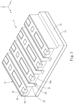
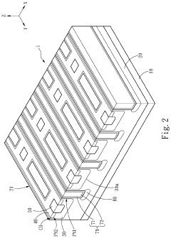
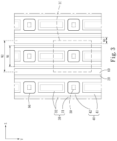
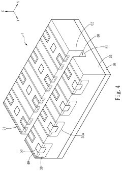
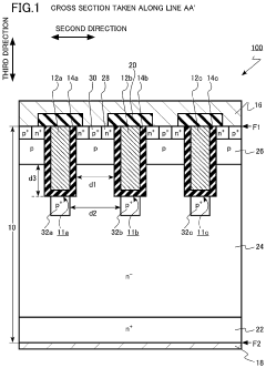
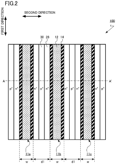
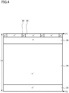
- A silicon carbide semiconductor device with a hybrid gate structure featuring a trench gate configuration that reduces JFET resistance and parasitic gate-to-drain capacitance, enhancing switching performance by increasing channel width density and optimizing the layout of doped regions and trenches.
Method of manufacturing semiconductor device and semiconductor device
PatentPendingUS20240088258A1
Innovation
- A method involving ion implantation of carbon and aluminum into specific regions of a silicon carbide layer, followed by heat treatment, to form carbon regions that suppress the diffusion of impurities and enhance the p-type impurity concentration in electric field relaxation regions, thereby reducing on-resistance and improving the reliability of the gate insulating layer.
Thermal Management Challenges and Solutions
Thermal management represents a critical challenge in the deployment of SiC MOSFETs and next-generation power devices. As power density increases in modern applications, the ability to efficiently dissipate heat becomes paramount for ensuring device reliability and performance. SiC MOSFETs, while offering superior thermal conductivity (approximately 3-4 times higher than silicon), still face significant thermal challenges when operating at high frequencies and power levels.
The junction temperature management of SiC devices presents unique difficulties compared to traditional silicon counterparts. While SiC can theoretically operate at temperatures exceeding 200°C (compared to silicon's typical 150°C limit), the packaging materials and interconnects often become the limiting factor. Current packaging technologies struggle to maintain reliability at these elevated temperatures, creating a bottleneck in fully leveraging SiC's thermal capabilities.
Advanced cooling solutions have emerged specifically tailored for SiC applications. Direct liquid cooling systems, which bring coolant closer to the die, have demonstrated up to 30% improvement in thermal resistance compared to conventional air cooling. Similarly, double-sided cooling techniques that extract heat from both sides of the device show promising results for high-power density applications, potentially reducing junction-to-ambient thermal resistance by 40-50%.
Novel thermal interface materials (TIMs) are being developed to address the thermal boundary resistance between SiC devices and heatsinks. Silver sintering and transient liquid phase bonding techniques have shown thermal conductivities 5-10 times higher than traditional solder materials, significantly improving heat transfer efficiency. These advanced TIMs are particularly crucial for SiC devices operating in harsh environments with frequent thermal cycling.
Thermal modeling and simulation tools have evolved to accurately predict hotspots and thermal gradients in SiC power modules. Multi-physics simulation approaches that couple electrical, thermal, and mechanical domains provide comprehensive insights into device behavior under various operating conditions. These tools enable designers to optimize layout, select appropriate cooling strategies, and predict reliability issues before physical prototyping.
When comparing SiC MOSFETs with emerging alternatives like GaN HEMTs or Ga2O3 devices, thermal management requirements differ significantly. While GaN devices typically operate at higher frequencies with lower power levels, their thermal conductivity is substantially lower than SiC, necessitating more aggressive cooling solutions. Conversely, diamond-based semiconductors offer superior thermal properties but remain commercially impractical due to manufacturing challenges and cost constraints.
Cost-Performance Tradeoffs in Next-Gen Power Electronics
The cost-performance balance represents a critical decision point for power electronics manufacturers and system designers when evaluating SiC MOSFETs against emerging alternatives. While SiC MOSFETs offer superior performance characteristics compared to traditional silicon devices, their higher manufacturing costs create significant market barriers, particularly in cost-sensitive applications.
Current SiC MOSFET pricing remains approximately 3-5 times higher than equivalent silicon devices, primarily due to substrate costs, manufacturing complexity, and lower production yields. This premium positioning limits widespread adoption in consumer electronics and automotive applications where bill-of-materials costs drive purchasing decisions. However, when evaluated through total cost of ownership models that include efficiency gains, reduced cooling requirements, and smaller passive components, SiC solutions demonstrate compelling long-term economic advantages in high-power applications.
Next-generation alternatives such as gallium nitride (GaN) and gallium oxide (Ga2O3) present different cost-performance profiles. GaN devices have seen rapid price reductions through innovative manufacturing approaches like GaN-on-silicon, potentially offering better cost trajectories than SiC in medium-voltage applications. Meanwhile, Ga2O3 remains primarily in research phases with promising theoretical performance but significant commercialization challenges.
Performance metrics reveal complex tradeoffs across device technologies. SiC MOSFETs excel in high-temperature operation (up to 200°C), high breakdown voltage (1.2kV-10kV range), and switching performance. GaN devices demonstrate superior high-frequency operation but face challenges in high-voltage applications. Diamond-based semiconductors offer theoretical performance advantages but remain prohibitively expensive for commercial deployment.
Market segmentation based on cost-performance requirements is emerging. High-performance, cost-insensitive applications like industrial drives, renewable energy systems, and grid infrastructure increasingly favor SiC solutions despite higher initial costs. Consumer and automotive markets show selective adoption patterns, implementing SiC only where performance advantages clearly justify cost premiums.
Manufacturing scale economies represent the primary pathway to improved cost-performance ratios. Industry projections suggest SiC device costs could decrease by 30-45% over the next five years as production volumes increase and manufacturing processes mature. This trajectory will likely accelerate SiC adoption across broader application categories while maintaining pressure on competing technologies to demonstrate clear value propositions.
Unlock deeper insights with Patsnap Eureka Quick Research — get a full tech report to explore trends and direct your research. Try now!
Generate Your Research Report Instantly with AI Agent
Supercharge your innovation with Patsnap Eureka AI Agent Platform!
