How Do SiC MOSFETs Impact Grid-Scale Energy Conversion?
SEP 8, 20259 MIN READ
Generate Your Research Report Instantly with AI Agent
Patsnap Eureka helps you evaluate technical feasibility & market potential.
SiC MOSFET Evolution and Efficiency Goals
Silicon Carbide (SiC) MOSFETs have undergone remarkable evolution since their commercial introduction in the early 2000s. Initially limited by high costs and manufacturing challenges, these wide bandgap semiconductors have steadily improved in performance metrics critical for grid-scale energy conversion applications. The technological trajectory has been characterized by continuous refinement in device structure, substrate quality, and fabrication processes, resulting in significant enhancements in switching speeds, thermal performance, and reliability.
The efficiency goals driving SiC MOSFET development are ambitious and multifaceted. Primary among these is the reduction of switching and conduction losses, which directly translates to higher power conversion efficiency. Current generation SiC MOSFETs demonstrate efficiency improvements of 2-3% over traditional silicon-based alternatives, a seemingly modest figure that represents substantial energy savings at grid scale. The industry roadmap targets achieving system-level efficiencies exceeding 99% in medium to high-voltage applications by 2025.
Another critical efficiency goal involves power density optimization. SiC MOSFETs enable operation at higher frequencies (typically 50-100 kHz compared to 5-20 kHz for silicon devices), allowing for smaller passive components and more compact converter designs. This translates to reduced material usage, smaller footprint requirements, and lower installation costs for grid infrastructure. Current targets aim for power density improvements of 300-400% compared to silicon-based systems.
Thermal management represents a third efficiency frontier. SiC's superior thermal conductivity (approximately 3-4 times that of silicon) and ability to operate reliably at junction temperatures up to 200°C (versus 150°C for silicon) enable simplified cooling systems and enhanced reliability under extreme conditions. The industry is working toward designs that can maintain optimal performance with reduced or passive cooling requirements, further improving system-level efficiency.
Reliability and operational lifetime constitute the fourth major efficiency goal. Grid infrastructure demands decades of consistent performance, and SiC MOSFETs are being engineered to meet these requirements. Current development focuses on gate oxide stability, package integrity under thermal cycling, and resistance to environmental stressors. The target is to achieve operational lifetimes exceeding 30 years with minimal performance degradation.
Cost efficiency remains perhaps the most challenging goal. Despite significant price reductions over the past decade, SiC MOSFETs still command a premium over silicon alternatives. The industry roadmap projects continued cost reduction through manufacturing scale improvements, yield optimization, and substrate size increases from current 6-inch to 8-inch wafers, with the aim of achieving cost parity with silicon IGBTs in grid applications by 2028-2030.
Grid-Scale Energy Conversion Market Analysis
The global grid-scale energy conversion market is experiencing significant growth, driven by the increasing demand for renewable energy integration and grid modernization. As of 2023, this market is valued at approximately $25 billion, with projections indicating a compound annual growth rate (CAGR) of 8.7% through 2030. The transition toward cleaner energy sources has accelerated investments in grid infrastructure upgrades, creating substantial opportunities for advanced power electronics solutions.
SiC MOSFETs are positioned to capture a growing share of this expanding market. Currently, silicon carbide devices represent about 5% of the total power semiconductor market in grid applications, but this share is expected to reach 15% by 2028. This growth is primarily driven by the superior efficiency and performance characteristics of SiC technology compared to traditional silicon-based solutions.
Regional analysis reveals varying adoption rates and market potentials. North America leads in SiC adoption for grid applications, accounting for approximately 38% of the global market share, followed by Europe at 32% and Asia-Pacific at 25%. China, in particular, has demonstrated aggressive growth in SiC implementation as part of its grid modernization initiatives, with investments exceeding $3 billion in 2022 alone.
The utility segment represents the largest end-user category, comprising about 45% of the total market. This is followed by renewable energy developers at 30% and industrial users at 20%. The remaining 5% consists of specialized applications such as microgrids and energy storage systems. The high-voltage segment (>1700V) is witnessing the fastest growth at 12% annually, reflecting the increasing deployment of SiC in high-power transmission and distribution systems.
Market drivers include stringent energy efficiency regulations, declining costs of SiC devices (approximately 15% reduction year-over-year), and the growing penetration of renewable energy sources in the global energy mix. Additionally, the push for grid resilience and reliability in the face of increasing extreme weather events has accelerated investments in advanced power electronics.
Challenges in market adoption include the higher initial cost compared to silicon alternatives, supply chain constraints for raw SiC materials, and the need for specialized expertise in system design and implementation. Despite these challenges, the value proposition of SiC MOSFETs in terms of system-level cost savings, reduced cooling requirements, and improved power density continues to drive market expansion.
SiC MOSFET Technology Status and Barriers
Silicon Carbide (SiC) MOSFETs represent a significant advancement in power semiconductor technology, offering superior performance characteristics compared to traditional silicon-based devices. Currently, SiC MOSFETs have reached commercial maturity for medium voltage applications (600V-1700V), with leading manufacturers such as Wolfspeed, ROHM, Infineon, and STMicroelectronics establishing reliable production capabilities.
Despite this progress, several technical barriers continue to impede the widespread adoption of SiC MOSFETs in grid-scale energy conversion systems. The most significant challenge remains the high manufacturing cost, with SiC devices typically commanding a 3-5x price premium over silicon counterparts. This cost differential stems from complex substrate production processes, lower manufacturing yields, and smaller wafer sizes compared to silicon technology.
Channel mobility represents another critical limitation, as SiC MOSFETs exhibit approximately 10 times lower mobility than silicon devices due to interface traps and defects at the SiC/SiO2 interface. This results in higher on-resistance and reduced efficiency, particularly at lower switching frequencies where the advantages of SiC are less pronounced.
Reliability concerns persist in high-temperature and high-voltage applications, with threshold voltage instability under gate bias stress conditions (bias temperature instability) remaining a significant issue. Additionally, the oxide reliability in SiC MOSFETs is compromised by higher electric fields at the semiconductor-oxide interface, leading to accelerated aging and potential premature failure in grid applications where operational lifetimes of 20+ years are expected.
Packaging technology presents another barrier, as traditional packaging solutions struggle to fully leverage SiC's high-temperature capabilities (potentially up to 200°C). Current commercial packages typically limit operation to 175°C, constraining the theoretical performance advantages of SiC materials.
From a geographical perspective, SiC MOSFET technology development is concentrated primarily in the United States, Japan, and Europe, with China rapidly increasing investments to reduce dependency on imported devices. This concentration creates supply chain vulnerabilities for grid infrastructure projects in regions without domestic production capabilities.
The scaling of SiC technology to higher voltage ratings (>3.3kV) necessary for direct grid-tied applications faces significant challenges in device design and manufacturing processes. While laboratory demonstrations have shown promising results for 10kV+ devices, commercial availability remains limited to lower voltage ratings, requiring complex cascaded topologies for grid-scale implementations.
Current SiC Implementation in Grid Applications
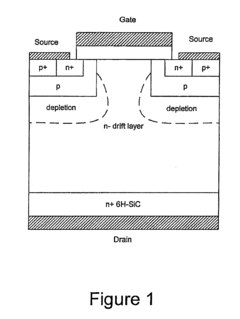
01 SiC MOSFET structure and fabrication for power conversion
Silicon Carbide (SiC) MOSFETs are designed with specific structural features to enhance power conversion efficiency. These include optimized gate structures, channel designs, and fabrication techniques that reduce on-resistance and switching losses. Advanced manufacturing processes help create more reliable SiC MOSFETs with improved thermal performance and higher breakdown voltages, making them ideal for high-efficiency energy conversion applications.- SiC MOSFET structure and fabrication for power conversion: Silicon Carbide (SiC) MOSFETs are designed with specific structural features to enhance power conversion efficiency. These include optimized gate structures, channel designs, and fabrication techniques that reduce on-resistance and switching losses. Advanced manufacturing processes improve the interface quality between SiC and gate oxide, resulting in higher reliability and performance in energy conversion applications.
- SiC MOSFET-based power conversion systems: Power conversion systems incorporating SiC MOSFETs offer significant advantages in energy efficiency and power density. These systems include DC-DC converters, inverters, and power supply units that leverage the high-temperature operation, fast switching capabilities, and low conduction losses of SiC technology. The implementation of SiC MOSFETs in these systems results in smaller form factors and reduced cooling requirements.
- Thermal management and reliability of SiC MOSFETs: Effective thermal management techniques are crucial for maximizing the performance and reliability of SiC MOSFETs in energy conversion applications. These include advanced packaging solutions, heat dissipation structures, and thermal interface materials that enable operation at higher temperatures. Reliability enhancement methods address issues such as gate oxide stability and threshold voltage shifts under high-temperature and high-field conditions.
- SiC MOSFET drivers and control strategies: Specialized gate driver circuits and control strategies are developed to fully exploit the capabilities of SiC MOSFETs in energy conversion. These include high-speed gate drivers with optimized turn-on and turn-off characteristics, protection circuits against voltage spikes, and advanced modulation techniques. The control strategies focus on minimizing switching losses while maintaining safe operation across various load conditions.
- Applications of SiC MOSFETs in renewable energy systems: SiC MOSFETs are increasingly deployed in renewable energy conversion systems such as solar inverters, wind power converters, and energy storage interfaces. Their high efficiency and high-frequency operation enable more compact and efficient power conversion in these applications. The implementation of SiC technology contributes to overall system efficiency improvements, reduced energy losses, and enhanced grid integration capabilities for renewable energy sources.
02 SiC MOSFET-based power conversion systems
Power conversion systems incorporating SiC MOSFETs offer significant advantages in energy efficiency and power density. These systems include DC-DC converters, inverters, and power supply units that leverage the fast switching capabilities and low conduction losses of SiC MOSFETs. The implementation of these devices in power conversion circuits results in smaller passive components, reduced cooling requirements, and overall system miniaturization while maintaining high efficiency.Expand Specific Solutions03 Thermal management for SiC MOSFETs in energy conversion
Effective thermal management is crucial for SiC MOSFETs in energy conversion applications. Various cooling techniques and packaging solutions are employed to dissipate heat efficiently from these high-power devices. Advanced thermal interface materials, optimized heat sink designs, and innovative cooling systems help maintain optimal operating temperatures, extending device lifetime and ensuring reliable performance under high-power conversion conditions.Expand Specific Solutions04 Gate drive optimization for SiC MOSFETs
Gate drive circuits specifically designed for SiC MOSFETs are essential for maximizing energy conversion efficiency. These circuits address the unique switching characteristics of SiC devices, including faster switching speeds and different threshold voltage requirements compared to silicon MOSFETs. Advanced gate drivers incorporate features like adjustable drive strength, protection mechanisms, and isolation techniques to optimize switching performance while ensuring reliable operation in high-power energy conversion applications.Expand Specific Solutions05 SiC MOSFETs in renewable energy conversion applications
SiC MOSFETs are increasingly deployed in renewable energy conversion systems such as solar inverters, wind power converters, and energy storage systems. Their high efficiency and ability to operate at elevated temperatures make them ideal for these applications. The implementation of SiC MOSFETs in renewable energy systems results in higher power conversion efficiency, reduced system size, and improved reliability, contributing to more effective harvesting and utilization of renewable energy sources.Expand Specific Solutions
Leading SiC MOSFET Manufacturers and Utilities
The SiC MOSFET market for grid-scale energy conversion is experiencing rapid growth, currently transitioning from early adoption to mainstream implementation. The market is projected to expand significantly as power grid modernization accelerates globally, with an estimated compound annual growth rate exceeding 25%. Technologically, SiC MOSFETs have reached commercial maturity, with key players demonstrating diverse levels of advancement. Wolfspeed leads with extensive SiC expertise, while established power electronics giants like Mitsubishi Electric, ROHM, Fuji Electric, and Infineon have developed comprehensive product portfolios. Chinese entities including Yangjie Electronic and CRRC Times Semiconductor are rapidly advancing their capabilities, while research institutions such as Xidian University and the Institute of Microelectronics of CAS are driving innovation through collaborative industry partnerships.
Mitsubishi Electric Corp.
Technical Solution: Mitsubishi Electric has developed advanced SiC MOSFET technology specifically optimized for grid-scale power conversion applications. Their latest generation devices feature a hybrid structure combining trench gates with planar cell designs, achieving on-resistance reduction of approximately 30% compared to conventional structures while maintaining short-circuit withstand capability exceeding 5μs at rated voltage. Mitsubishi's SiC technology incorporates proprietary edge termination structures that enhance surge capability, critical for grid applications experiencing lightning strikes and switching transients. Their full SiC power modules rated up to 3.3kV and 1500A feature optimized internal layouts with balanced current distribution and reduced parasitic inductance below 15nH. For grid applications, Mitsubishi has demonstrated that replacing silicon IGBTs with SiC MOSFETs in medium-voltage converters can reduce switching losses by up to 75% and increase power density by 250%. Their technology has been deployed in HVDC converter stations, demonstrating efficiency improvements of 1.8% at system level, which translates to energy savings of approximately 15.8 GWh annually for a 1GW installation.
Strengths: Extensive experience in high-power applications; comprehensive power module portfolio with integrated cooling solutions; proven field reliability in utility-scale deployments. Weaknesses: Higher initial cost compared to silicon alternatives; requires specialized gate driver designs with precise timing control; thermal cycling capability still being optimized for the most demanding grid applications.
ROHM Co., Ltd.
Technical Solution: ROHM has developed a comprehensive SiC MOSFET portfolio specifically engineered for grid-scale energy conversion applications. Their 4th generation SiC MOSFETs feature a proprietary double-trench structure that simultaneously reduces on-resistance by approximately 40% and gate charge by 35% compared to conventional designs. ROHM's technology incorporates a unique gate oxide formation process that enhances reliability under high-temperature operation, demonstrating stable performance after 1000 hours at 175°C with gate bias stress. For grid applications, ROHM has implemented advanced termination structures that provide surge capability exceeding 1.2x the rated breakdown voltage, critical for handling grid transients. Their SiC solutions have been deployed in utility-scale solar inverters, demonstrating efficiency improvements of 2.5% compared to silicon-based designs, which translates to approximately 50MWh of additional energy production annually for a 100MW installation. ROHM's integrated SiC power modules feature optimized internal layouts that reduce parasitic inductance to below 10nH, enabling switching frequencies above 100kHz in grid-tied applications.
Strengths: Vertically integrated manufacturing from substrate to finished device ensures quality control; comprehensive design support including simulation models and reference designs; established volume production with demonstrated reliability. Weaknesses: More limited power module portfolio compared to some competitors; higher cost structure for lower volume applications; requires specialized gate drive circuits to fully optimize switching performance.
Critical SiC MOSFET Design Innovations
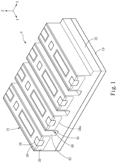
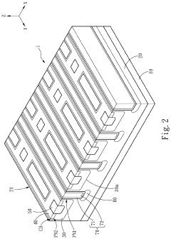
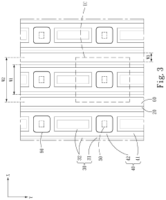
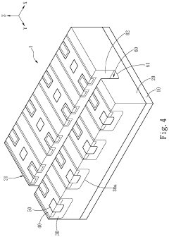
Silicon carbide semiconductor device
PatentPendingUS20240234569A9
Innovation
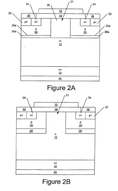
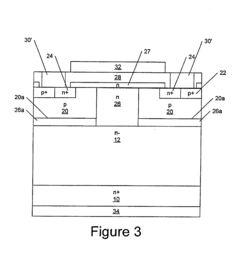
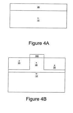
- A silicon carbide semiconductor device with a hybrid gate structure featuring a trench gate configuration that reduces JFET resistance and parasitic gate-to-drain capacitance, enhancing switching performance by increasing channel width density and optimizing the layout of doped regions and trenches.
Silicon carbide power MOS field effect transistors
PatentInactiveEP2383787A1
Innovation
- The implementation of an n-type silicon carbide limiting region with a higher carrier concentration than the drift layer, positioned between the drift layer and the p-type silicon carbide region, reduces the depletion region and on-state resistance by creating a shorter current path and alleviating the JFET resistance issues, while also utilizing an epitaxial layer or implanted regions to enhance mobility.
Thermal Management Challenges
Silicon Carbide (SiC) MOSFETs present significant thermal management challenges in grid-scale energy conversion applications despite their superior performance characteristics. These devices generate substantial heat during high-power operation, with junction temperatures potentially reaching 175-200°C under full load conditions. This thermal stress necessitates advanced cooling solutions beyond traditional silicon-based systems, as SiC components can operate at higher temperatures but still require effective heat dissipation to maintain reliability and performance.
The power density increase enabled by SiC MOSFETs creates concentrated heat zones within conversion equipment, requiring redesigned thermal interfaces and heat spreading techniques. Conventional thermal interface materials often prove inadequate for the thermal conductivity demands of SiC-based power converters, leading to the development of specialized materials with enhanced thermal properties specifically engineered for wide-bandgap semiconductor applications.
Thermal cycling presents another critical challenge, particularly in grid applications where load profiles fluctuate throughout daily operation cycles. The coefficient of thermal expansion mismatch between SiC dies and packaging materials creates mechanical stress during temperature variations, potentially leading to package delamination, wire bond fatigue, or solder joint degradation over time. This necessitates careful material selection and packaging design to ensure long-term reliability in field deployments.
Cooling system architecture must be fundamentally reconsidered for SiC implementations. While liquid cooling offers superior thermal performance necessary for high-power density applications, it introduces complexity, maintenance requirements, and potential reliability concerns. Air-cooled solutions remain preferable for certain deployments but require optimization through computational fluid dynamics modeling to ensure adequate airflow across critical components.
Temperature monitoring and thermal protection mechanisms require greater sophistication in SiC-based systems. The faster switching speeds and higher operational temperatures demand more responsive thermal protection circuits with appropriate temperature sensors strategically placed to detect hotspots before they cause device failure. Advanced gate drivers with integrated temperature sensing and protection features are becoming essential components in SiC MOSFET implementations.
Cost-performance optimization presents perhaps the most significant challenge for system designers. While more elaborate cooling solutions enable SiC MOSFETs to operate at peak performance, they add cost and complexity to the overall system. Finding the optimal balance between thermal management investment and performance gains requires sophisticated modeling and thorough understanding of application-specific requirements to maximize the value proposition of SiC technology in grid-scale energy conversion systems.
Grid Reliability and Resilience Implications
The integration of Silicon Carbide (SiC) MOSFETs into grid-scale energy conversion systems significantly enhances grid reliability and resilience through multiple technical advantages. These wide-bandgap semiconductor devices demonstrate superior performance under extreme conditions, maintaining operational stability at temperatures exceeding 200°C while conventional silicon-based components typically fail beyond 150°C. This temperature tolerance directly translates to more robust grid infrastructure that can withstand thermal stress during demand surges or adverse weather conditions.
SiC MOSFETs contribute to grid resilience through their exceptional switching capabilities, which reduce energy losses by up to 50% compared to traditional silicon alternatives. This efficiency improvement minimizes heat generation within power conversion equipment, substantially decreasing the likelihood of thermal-related failures that often cascade into wider grid disruptions. The reduced cooling requirements also simplify system designs, eliminating potential points of failure in thermal management systems.
The inherent radiation hardness of SiC devices provides critical protection against electromagnetic pulses and solar events that can devastate conventional grid infrastructure. This characteristic becomes increasingly valuable as grid systems face growing threats from space weather phenomena and potential electromagnetic interference sources. Power conversion systems utilizing SiC MOSFETs can maintain operation through disturbances that would otherwise trigger widespread outages.
From a grid architecture perspective, SiC-based converters enable more flexible and responsive power flow control. Their higher switching frequencies support advanced grid-stabilizing functions like reactive power compensation and harmonic filtering with unprecedented speed and precision. This capability allows grid operators to maintain power quality parameters within tighter tolerances, preventing equipment damage across the network and extending infrastructure lifespan.
The reliability improvements manifest in quantifiable metrics, with SiC-based systems demonstrating mean time between failures (MTBF) rates 2-3 times higher than silicon equivalents in field deployments. This translates directly to fewer service interruptions and reduced maintenance requirements. The extended operational lifetime of SiC components—typically 15-20 years versus 8-12 years for traditional solutions—further enhances long-term grid stability and reduces lifecycle costs.
For critical infrastructure protection, SiC MOSFETs enable more effective fault isolation and faster system recovery. Their rapid switching capabilities allow protective circuits to respond to fault conditions in microseconds rather than milliseconds, containing potential cascading failures before they propagate through the grid. This characteristic proves especially valuable in microgrids and islanded systems where resilience against external disruptions is paramount.
Unlock deeper insights with Patsnap Eureka Quick Research — get a full tech report to explore trends and direct your research. Try now!
Generate Your Research Report Instantly with AI Agent
Supercharge your innovation with Patsnap Eureka AI Agent Platform!