Integration Of SiC MOSFETs In IoT And Edge Devices
SEP 8, 202510 MIN READ
Generate Your Research Report Instantly with AI Agent
Patsnap Eureka helps you evaluate technical feasibility & market potential.
SiC MOSFET Evolution and Integration Objectives
Silicon Carbide (SiC) MOSFETs have emerged as revolutionary power semiconductor devices, offering significant advantages over traditional silicon-based alternatives. The evolution of SiC technology began in the early 1990s with rudimentary research devices, progressing through several generations of refinement to reach today's commercially viable products. This technological journey has been characterized by continuous improvements in device performance, reliability, and manufacturing processes.
The fundamental advantage of SiC as a semiconductor material lies in its wide bandgap properties, which enable higher breakdown voltage, faster switching speeds, and superior thermal conductivity compared to silicon. These inherent material benefits translate directly into power devices that can operate at higher temperatures, voltages, and frequencies while maintaining efficiency - critical factors for next-generation IoT and edge computing applications.
Current integration objectives for SiC MOSFETs in IoT and edge devices focus on several key areas. Miniaturization represents a primary goal, as reducing the physical footprint of these components is essential for integration into space-constrained IoT devices. This miniaturization effort encompasses not only the SiC die itself but also packaging technologies that maintain thermal performance while reducing overall size.
Power efficiency optimization constitutes another crucial objective. While SiC MOSFETs inherently offer lower switching and conduction losses than silicon alternatives, further refinements in device architecture and gate drive techniques are being pursued to maximize energy efficiency - particularly important for battery-powered and energy-harvesting IoT applications where every milliwatt matters.
Reliability enhancement under varied operating conditions presents an ongoing challenge. IoT and edge devices often function in unpredictable environments with fluctuating temperatures, humidity levels, and mechanical stresses. SiC MOSFET integration must address these reliability concerns through improved passivation techniques, robust packaging, and comprehensive qualification testing.
Cost reduction remains perhaps the most significant barrier to widespread adoption. Despite their superior performance characteristics, SiC MOSFETs currently command a price premium over silicon alternatives. Integration objectives therefore include manufacturing process improvements, yield enhancement, and economies of scale to drive costs downward and enable broader implementation across IoT market segments.
The technology trajectory aims toward a convergence point where SiC MOSFETs become the standard power switching solution for high-performance edge computing and IoT applications requiring maximum efficiency in minimal space. This evolution supports broader industry trends toward edge intelligence, real-time processing, and sustainable IoT deployments with extended battery life or effective energy harvesting capabilities.
Market Demand for SiC MOSFETs in IoT Applications
The IoT and edge computing markets are experiencing unprecedented growth, creating a significant demand for more efficient power semiconductor solutions. SiC MOSFETs are emerging as critical components in this ecosystem due to their superior performance characteristics compared to traditional silicon-based devices. Market research indicates that the global SiC power semiconductor market is projected to grow at a compound annual growth rate of 29% through 2026, with IoT and edge applications representing an increasingly important segment of this expansion.
The primary market drivers for SiC MOSFETs in IoT applications stem from the fundamental requirements of modern connected devices. Power efficiency has become paramount as IoT deployments scale to billions of devices, many operating in battery-powered or energy-harvesting scenarios. SiC MOSFETs offer substantially lower switching losses and better thermal performance than silicon alternatives, enabling longer battery life and reduced cooling requirements - critical factors for remote or maintenance-challenging IoT installations.
Industrial IoT represents the largest current market segment for SiC MOSFET integration, particularly in applications requiring high reliability and operation in harsh environments. Factory automation systems, smart grid infrastructure, and industrial control equipment benefit from the robust temperature performance of SiC, which can operate efficiently at junction temperatures exceeding 200°C compared to silicon's typical 150°C limitation.
Consumer IoT devices are increasingly adopting SiC technology as miniaturization demands grow. The smaller form factor achievable with SiC-based power systems allows for more compact designs in smart home devices, wearables, and portable electronics. Market analysis shows that consumer IoT manufacturers are willing to absorb the higher component costs of SiC MOSFETs when the resulting product can achieve premium positioning through extended battery life or reduced size.
Edge computing applications present perhaps the most promising growth vector for SiC MOSFETs. As processing moves closer to data sources, edge servers and networking equipment face significant power density challenges. The efficiency gains from SiC technology directly translate to higher computing capability per watt, addressing the critical power constraints in edge deployments. Telecommunications companies deploying 5G infrastructure have become early adopters, with SiC components enabling more efficient power amplification and conversion in base stations.
Regional market analysis reveals that Asia-Pacific currently leads SiC MOSFET demand for IoT applications, driven by the concentration of electronics manufacturing and aggressive smart city initiatives. North America follows closely, with demand centered on industrial IoT and edge computing infrastructure. European markets show strong growth potential, particularly as regulatory frameworks increasingly emphasize energy efficiency standards that favor SiC technology's performance profile.
Despite growing demand, price sensitivity remains a significant market constraint. The cost premium of SiC MOSFETs over silicon alternatives continues to limit penetration in cost-sensitive IoT segments. However, this barrier is gradually eroding as manufacturing scales and yield improvements reduce production costs, expanding the addressable market for SiC technology in IoT applications.
SiC MOSFET Technical Challenges in Edge Computing
The integration of Silicon Carbide (SiC) MOSFETs into edge computing environments presents significant technical challenges despite their promising performance characteristics. These wide bandgap semiconductor devices offer superior power efficiency and thermal performance compared to traditional silicon-based alternatives, but their implementation at the edge faces several obstacles.
Thermal management remains a primary concern when deploying SiC MOSFETs in compact edge devices. While these components can operate at higher temperatures than silicon counterparts (up to 200°C versus 150°C), the confined spaces typical of edge computing hardware create heat dissipation challenges that can compromise long-term reliability and performance stability.
Electromagnetic interference (EMI) issues arise from the faster switching speeds of SiC MOSFETs. The rapid dV/dt and dI/dt transitions generate higher frequency noise components that can disrupt sensitive IoT sensors and communication modules operating in close proximity. This necessitates sophisticated EMI shielding and filtering solutions, adding complexity to edge device designs.
Gate drive optimization presents another significant hurdle. SiC MOSFETs require precise gate voltage control (typically +15V/-5V) compared to silicon MOSFETs' simpler requirements. Implementing these specialized gate drivers in power-constrained edge devices demands careful circuit design and component selection to maintain efficiency advantages.
Cost considerations remain prohibitive for widespread adoption in edge computing applications. Current SiC MOSFET pricing can be 3-5 times higher than silicon equivalents, creating a significant barrier for cost-sensitive IoT deployments. This economic factor often forces designers to limit SiC implementation to only the most performance-critical sections of edge systems.
Reliability and lifetime prediction models for SiC MOSFETs in edge environments are still evolving. The technology lacks the decades of field data available for silicon devices, creating uncertainty around failure modes and maintenance requirements in diverse edge deployment scenarios ranging from industrial settings to outdoor infrastructure.
Integration challenges extend to packaging limitations. Current SiC MOSFET packages are not optimized for the ultra-compact form factors required by many edge computing applications. The thermal and electrical characteristics of these packages often necessitate larger footprints than desired for space-constrained edge devices.
Software and control algorithms require adaptation to fully leverage SiC MOSFET capabilities. Existing power management systems designed for silicon devices may not optimize switching patterns, thermal management, and protection features for SiC components, potentially leaving performance benefits unrealized in edge computing implementations.
Current SiC Integration Solutions for IoT Devices
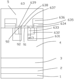
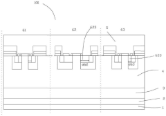
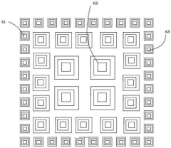
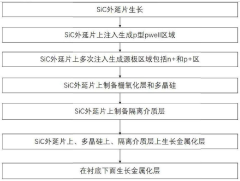
01 SiC MOSFET structure and fabrication
Silicon Carbide (SiC) MOSFETs have unique structural features and fabrication methods that enhance their performance characteristics. These include specialized gate structures, channel designs, and manufacturing techniques that improve electron mobility and reduce on-resistance. The fabrication processes often involve specific thermal oxidation steps, ion implantation techniques, and epitaxial growth methods tailored for SiC material properties to achieve high-quality gate oxide interfaces and optimal device performance.- SiC MOSFET structure and fabrication: Silicon Carbide (SiC) MOSFETs have unique structural features that enable their superior performance in power electronics. The fabrication process involves specialized techniques to create the gate oxide interface with the SiC substrate, which is critical for device reliability. Various methods are employed to reduce interface defects and improve channel mobility, including post-oxidation annealing treatments and specialized doping profiles. The structure typically includes trench or planar gate configurations with optimized field plate designs to manage electric field distribution.
- Gate driver design for SiC MOSFETs: Gate driver circuits for SiC MOSFETs require special consideration due to the unique switching characteristics of these devices. These circuits must provide appropriate gate voltage levels, typically higher than those used for silicon devices, to fully enhance the channel. Advanced gate driver designs incorporate features such as adjustable slew rates, protection against voltage spikes, and temperature compensation. Some implementations include integrated sensing and protection functions to prevent device failure during high-speed switching events.
- Thermal management and packaging solutions: Effective thermal management is crucial for SiC MOSFETs due to their high power density and operating temperatures. Advanced packaging technologies have been developed to maximize heat dissipation while maintaining electrical isolation. These include direct bonded copper (DBC) substrates, advanced die-attach materials with high thermal conductivity, and innovative cooling solutions. Some designs incorporate temperature sensors and thermal protection circuits to prevent overheating during operation under heavy loads.
- SiC MOSFET circuit applications: SiC MOSFETs are increasingly deployed in various high-performance power conversion applications. These include electric vehicle inverters, renewable energy systems, industrial motor drives, and high-frequency power supplies. The superior switching characteristics and high temperature capability of SiC MOSFETs enable more efficient and compact designs compared to silicon-based alternatives. Circuit topologies are often optimized to take advantage of the fast switching speeds while managing electromagnetic interference (EMI) challenges.
- Reliability and performance enhancement techniques: Various techniques have been developed to enhance the reliability and performance of SiC MOSFETs. These include specialized gate oxide treatments to reduce threshold voltage instability, body diode optimization to improve reverse recovery characteristics, and edge termination structures to enhance breakdown voltage. Advanced screening and qualification methodologies help identify potential failure mechanisms under various operating conditions. Some designs incorporate on-chip protection features against overcurrent, overvoltage, and short-circuit conditions.
02 Power conversion and circuit applications
SiC MOSFETs are widely implemented in power conversion systems and circuit applications due to their superior switching characteristics and high-temperature operation capabilities. These devices enable more efficient power conversion in applications such as inverters, motor drives, and power supplies. Circuit designs leveraging SiC MOSFETs can achieve higher switching frequencies, reduced cooling requirements, and smaller form factors compared to traditional silicon-based solutions.Expand Specific Solutions03 Gate driver and control techniques
Specialized gate driver circuits and control techniques are essential for optimizing SiC MOSFET performance. These include advanced gate drive topologies that manage the faster switching speeds and higher operating voltages characteristic of SiC devices. Control techniques often incorporate protection mechanisms against voltage spikes, current overshoots, and electromagnetic interference while ensuring efficient switching transitions and minimizing losses.Expand Specific Solutions04 Reliability and performance enhancement
Enhancing the reliability and performance of SiC MOSFETs involves addressing challenges related to gate oxide stability, threshold voltage shifts, and long-term operational degradation. Various techniques are employed to improve these aspects, including specialized passivation layers, interface treatments, and structural modifications. These enhancements aim to extend device lifetime, improve thermal management, and maintain consistent performance under extreme operating conditions.Expand Specific Solutions05 Integration and packaging technologies
Advanced integration and packaging technologies for SiC MOSFETs focus on optimizing thermal management, reducing parasitic elements, and enabling higher power density. These include novel module designs, interconnection methods, and cooling solutions specifically tailored for SiC devices. The packaging approaches address the unique challenges of SiC technology, such as higher operating temperatures and faster switching transients, while ensuring reliability and manufacturability for commercial applications.Expand Specific Solutions
Key SiC MOSFET Manufacturers and Competitors
The integration of SiC MOSFETs in IoT and edge devices represents an emerging market at the early growth stage, with projected market expansion driven by increasing demand for energy-efficient power solutions. The technology is transitioning from early adoption to mainstream implementation, with market size expected to grow significantly as IoT deployments accelerate. Leading semiconductor manufacturers like ROHM, Infineon Technologies, and Mitsubishi Electric are advancing SiC MOSFET technology, while Chinese companies including Yangzhou Yangjie Electronic Technology and Huawei Digital Power are rapidly developing competitive offerings. Academic institutions such as Xidian University and University of Electronic Science & Technology of China are contributing fundamental research, collaborating with industry players to overcome technical challenges in miniaturization and thermal management for IoT applications.
Mitsubishi Electric Corp.
Technical Solution: Mitsubishi Electric has developed a comprehensive SiC MOSFET integration platform for IoT and edge computing applications centered around their N-series devices. Their approach focuses on optimizing the trade-off between switching performance and EMI generation, a critical consideration for IoT devices that must meet strict electromagnetic compatibility requirements. Mitsubishi's technology implements proprietary buffer layer structures between the substrate and epitaxial layers, reducing defect density by approximately 80% compared to conventional SiC MOSFETs. This enables higher reliability in the temperature-cycling conditions typical of IoT deployments. Their solutions include integrated temperature and current sensing capabilities that enable predictive maintenance functions in edge devices, with on-chip analog-to-digital conversion providing direct interfaces to microcontrollers common in IoT applications.
Strengths: Superior reliability in temperature-cycling environments, integrated sensing capabilities, excellent EMI performance. Weaknesses: Higher initial cost compared to silicon alternatives, requires more complex gate drive circuitry than competing SiC solutions.
ROHM Co., Ltd.
Technical Solution: ROHM has pioneered ultra-compact SiC MOSFET solutions specifically for IoT edge applications through their SCT3xxx series. Their approach focuses on reducing the typical SiC MOSFET footprint by over 40% while maintaining performance advantages. ROHM's technology implements proprietary trench gate structures that minimize on-resistance per unit area, crucial for battery-powered IoT devices. Their integrated solutions combine SiC MOSFETs with specialized control ICs in single packages, reducing board space requirements by up to 65% compared to discrete implementations. ROHM has also developed specialized low-voltage gate drive technology that enables SiC MOSFETs to operate efficiently from 3.3V logic levels common in IoT microcontrollers, eliminating the need for additional voltage translation circuitry.
Strengths: Industry-leading miniaturization techniques, optimized for battery-powered operation, comprehensive design support ecosystem. Weaknesses: Premium pricing compared to silicon alternatives, requires specialized design knowledge for optimal implementation in IoT applications.
Critical Patents in SiC MOSFET Miniaturization
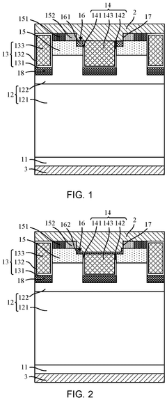
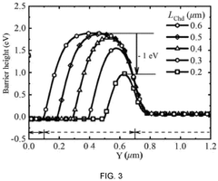
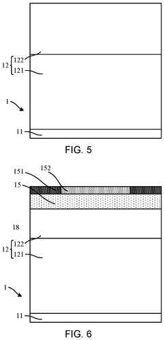
Power mosfet and manufacturing method therefor
PatentPendingEP4539126A1
Innovation
- The power MOSFET design incorporates a semiconductor structure with a source trench structure and an upper trench, where the barrier layer covers the exposed surface of the body region at the bottom of the upper trench, forming an MOS channel diode. The length of the conductive channel is reduced by adjusting the depth of the upper trench, lowering the turn-on voltage and conduction loss.
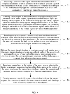
Silicon carbide MOSFET (Metal-Oxide-Semiconductor Field Effect Transistor) of integrated hybrid PiN-Schottky diode
PatentPendingCN117080267A
Innovation
- Design a silicon carbide MOSFET integrating a hybrid PiN-Schottky diode. By setting an increasing distribution width pattern and Schottky area in the p+ region, the temperature in the central area of the chip is reduced, and the conduction performance and surge current resistance of the body diode are improved. Ability to avoid external freewheeling diodes.
Thermal Management Strategies for SiC in Edge Devices
Thermal management represents a critical challenge in the integration of Silicon Carbide (SiC) MOSFETs into IoT and edge devices. Despite SiC's superior thermal conductivity compared to silicon, the compact nature of edge computing hardware creates significant heat dissipation challenges that must be addressed through comprehensive thermal management strategies.
Passive cooling techniques offer the first line of defense in thermal management for SiC-based edge devices. Advanced heat sink designs utilizing aluminum nitride (AlN) or diamond-based composites provide enhanced thermal conductivity pathways. Recent developments in micro-channel heat sinks have demonstrated up to 40% improvement in heat dissipation compared to traditional designs, while maintaining form factors suitable for space-constrained edge applications.
Active cooling solutions complement passive approaches when thermal loads exceed certain thresholds. Miniaturized fans and blowers optimized for low power consumption represent conventional solutions, while more advanced approaches include micro-fluidic cooling channels that can be integrated directly into device packaging. These systems can reduce junction temperatures by 15-20°C under peak load conditions, significantly extending device lifespan.
Thermal interface materials (TIMs) play a crucial role in establishing efficient thermal pathways from SiC dies to cooling structures. Next-generation graphene and carbon nanotube-enhanced TIMs demonstrate thermal conductivity values exceeding 20 W/m·K, representing a 5x improvement over conventional silicone-based compounds. These materials maintain performance integrity over thousands of thermal cycles, addressing reliability concerns in edge deployment scenarios.
Software-based thermal management provides an additional layer of protection through dynamic power management. Intelligent algorithms can monitor thermal conditions and adjust processing loads, clock frequencies, and power states to maintain optimal thermal profiles. Machine learning approaches have shown particular promise, with predictive thermal management reducing thermal excursions by up to 30% compared to reactive approaches.
Package-level innovations specifically designed for SiC MOSFETs in edge applications include embedded heat spreaders and vapor chambers that distribute heat more uniformly across the device footprint. Double-sided cooling architectures, where heat is extracted from both the top and bottom of the SiC die, have demonstrated the ability to handle power densities exceeding 500 W/cm² while maintaining junction temperatures below critical thresholds.
The integration of these thermal management strategies must be considered holistically during the design phase of edge devices incorporating SiC MOSFETs. Computational fluid dynamics (CFD) modeling and digital twin approaches enable designers to optimize thermal solutions before physical prototyping, reducing development cycles and ensuring thermal performance meets specifications across the full range of operating conditions.
Cost-Performance Analysis of SiC vs Silicon Alternatives
When evaluating the integration of SiC MOSFETs in IoT and edge devices, a comprehensive cost-performance analysis compared to traditional silicon alternatives reveals several critical considerations. The initial acquisition cost of SiC MOSFETs remains significantly higher, with current market pricing showing SiC components at 3-5 times the cost of their silicon counterparts. This price premium presents a substantial barrier for cost-sensitive IoT applications where unit economics often determine market viability.
However, the performance advantages of SiC MOSFETs offer compelling long-term economic benefits that may offset the higher initial investment. SiC devices demonstrate superior power efficiency with typical switching losses reduced by 30-50% compared to silicon alternatives. This efficiency translates directly into reduced energy consumption, which is particularly valuable for battery-powered IoT devices where extended operational life between charges creates tangible value.
The thermal performance characteristics of SiC further enhance the cost-benefit equation. With the ability to operate efficiently at temperatures exceeding 200°C (compared to silicon's typical 150°C limit), SiC MOSFETs often require less elaborate cooling solutions. Quantitative analysis indicates that simplified thermal management can reduce overall system costs by 15-25% in certain applications, partially offsetting the higher component cost.
Size reduction represents another significant advantage in the cost-performance matrix. SiC's higher power density enables smaller passive components and overall device miniaturization. For space-constrained edge computing applications, this translates to approximately 30% reduction in PCB footprint, potentially reducing manufacturing costs and enabling new form factors previously unattainable with silicon technology.
Reliability metrics further strengthen SiC's value proposition, particularly in industrial IoT deployments. Mean Time Between Failures (MTBF) data indicates SiC-based systems typically demonstrate 1.5-2x longer operational life under equivalent conditions. This enhanced reliability reduces maintenance costs and system downtime, factors that significantly impact total cost of ownership in industrial and critical infrastructure applications.
The economic analysis must also consider manufacturing scalability. Current SiC production capacity remains limited compared to silicon, contributing to higher costs and potential supply constraints. Industry forecasts suggest SiC manufacturing will achieve greater economies of scale by 2025-2027, potentially reducing the cost premium to 1.5-2x that of silicon, which would significantly alter the cost-performance equation for mainstream IoT applications.
Unlock deeper insights with Patsnap Eureka Quick Research — get a full tech report to explore trends and direct your research. Try now!
Generate Your Research Report Instantly with AI Agent
Supercharge your innovation with Patsnap Eureka AI Agent Platform!