OLED vs MicroLED: Protective Coating Advancements
OCT 24, 20259 MIN READ
Generate Your Research Report Instantly with AI Agent
Patsnap Eureka helps you evaluate technical feasibility & market potential.
OLED and MicroLED Coating Evolution and Objectives
The evolution of display technologies has witnessed significant advancements over the past two decades, with OLED (Organic Light Emitting Diode) emerging as a dominant technology since the early 2000s. OLED displays revolutionized the industry with their self-emissive properties, eliminating the need for backlighting and enabling thinner, more flexible displays with superior contrast ratios and color reproduction. The technology's trajectory has been marked by continuous improvements in efficiency, lifetime, and manufacturing processes.
More recently, MicroLED has emerged as a promising next-generation display technology, offering potential advantages over OLED in brightness, energy efficiency, and longevity. First demonstrated in laboratory settings in the early 2010s, MicroLED utilizes inorganic semiconductor materials to create arrays of microscopic LEDs that function as individual pixels. This fundamental difference in materials science presents both opportunities and challenges in protective coating requirements.
Protective coatings serve as critical components in both display technologies, though their functions and compositions differ significantly. For OLEDs, coatings primarily address the organic materials' vulnerability to oxygen and moisture, which can cause rapid degradation of display performance. The evolution of OLED protective coatings has progressed from early glass encapsulation methods to advanced thin-film encapsulation (TFE) technologies incorporating multiple inorganic and organic layers.
MicroLED protective coatings, while sharing some functional requirements with OLED coatings, must address distinct challenges related to the inorganic nature of the emitters and the unique manufacturing processes involved. The development trajectory for MicroLED coatings has focused on maintaining optical performance while providing mechanical protection during the complex transfer and integration processes required for manufacturing.
The technical objectives for advancing protective coatings in both technologies converge around several key parameters: enhanced barrier properties against environmental factors, improved optical transparency, increased mechanical flexibility, and cost-effective manufacturing scalability. For OLEDs, extending operational lifetime through superior moisture barriers remains paramount, while MicroLED coating development aims to optimize light extraction efficiency and enable novel form factors.
Industry roadmaps indicate that future coating technologies will increasingly incorporate nanomaterials and atomic layer deposition techniques to achieve unprecedented performance metrics. Research efforts are targeting coatings that not only protect but actively enhance display performance through properties such as anti-reflection, self-healing capabilities, and enhanced thermal management. The convergence of materials science, nanotechnology, and advanced manufacturing processes is expected to yield transformative coating solutions for both display technologies in the coming years.
Market Demand Analysis for Advanced Display Protection
The global market for advanced display protection technologies is experiencing robust growth, driven primarily by the expanding consumer electronics sector and increasing adoption of premium display technologies. As OLED and emerging MicroLED displays gain market share, the demand for specialized protective coatings has intensified significantly. Current market analysis indicates that the display protection market is expected to grow at a compound annual growth rate of 15.3% through 2028, with protective coatings representing a substantial segment of this expansion.
Consumer expectations regarding display durability have evolved dramatically in recent years. End-users now demand displays that can withstand daily wear and tear while maintaining optical clarity and touch sensitivity. This shift has created a substantial market opportunity for advanced protective solutions that can address the unique vulnerabilities of OLED and MicroLED technologies. Particularly, protection against moisture ingress, oxygen penetration, and mechanical damage represents critical concerns for manufacturers and consumers alike.
The smartphone segment continues to dominate demand for advanced display protection, accounting for approximately 65% of the total market. However, emerging applications in wearable technology, automotive displays, and foldable devices are rapidly expanding market boundaries. The foldable display segment specifically has created unprecedented challenges for protective coating technologies, requiring solutions that maintain flexibility while providing adequate protection against environmental factors.
Regional analysis reveals that Asia-Pacific currently leads the market for advanced display protection, with China, South Korea, and Japan serving as manufacturing hubs for display technologies. North America and Europe follow as significant markets, driven by high consumer purchasing power and early technology adoption. Developing economies in Southeast Asia and Latin America represent emerging markets with substantial growth potential as smartphone penetration increases.
Price sensitivity varies significantly across market segments. While premium smartphone manufacturers prioritize performance over cost, mid-range device makers seek cost-effective solutions that provide adequate protection without significantly impacting retail prices. This bifurcation has led to the development of tiered protective coating solutions catering to different market segments.
Industry surveys indicate that consumers increasingly consider display durability as a key purchasing factor, with 78% of respondents citing screen damage as a major concern when selecting electronic devices. This consumer awareness has translated into willingness to pay premium prices for devices with enhanced protection features, creating additional market incentives for manufacturers to invest in advanced protective technologies.
Current Protective Coating Technologies and Limitations
Both OLED and MicroLED display technologies require sophisticated protective coatings to ensure longevity and performance. Current protective coating technologies for these displays can be categorized into several types, each with specific advantages and limitations.
Thin-film encapsulation (TFE) represents the most widely adopted protective solution for OLED displays. This technology utilizes alternating layers of inorganic materials (typically silicon nitride or aluminum oxide) and organic materials to create a barrier against moisture and oxygen. While TFE offers excellent barrier properties with water vapor transmission rates (WVTR) as low as 10^-6 g/m²/day, it faces challenges in manufacturing scalability and cost-effectiveness for larger display formats.
Atomic Layer Deposition (ALD) has emerged as a premium coating method that provides exceptional conformality and precise thickness control down to the atomic level. ALD coatings deliver superior moisture barriers but suffer from extremely slow deposition rates, significantly impacting production throughput and increasing manufacturing costs. This limitation has restricted ALD's widespread adoption despite its technical superiority.
For MicroLED displays, traditional glass encapsulation remains common but adds considerable weight and limits design flexibility. Recent advancements have introduced hybrid approaches combining glass with polymer adhesives, though these solutions still struggle with optical clarity maintenance over extended periods.
Parylene conformal coatings offer another alternative, providing excellent chemical resistance and dielectric properties. However, their application process requires specialized vacuum equipment and presents challenges in achieving uniform coverage across complex display architectures, particularly for MicroLED's intricate structures.
Nanocomposite coatings incorporating materials such as graphene oxide or ceramic nanoparticles show promising barrier properties but face reproducibility issues in large-scale manufacturing environments. Consistency in dispersion and adhesion remains problematic when scaling from laboratory to production environments.
A significant limitation across all current technologies is the trade-off between barrier performance and optical properties. Higher barrier performance often comes at the cost of reduced light transmission or increased haze, directly impacting display quality. This compromise becomes particularly critical for MicroLED displays, where light efficiency is paramount.
Temperature sensitivity presents another major challenge, as many coating processes require conditions that can damage temperature-sensitive OLED materials. MicroLED displays offer greater thermal stability but still require careful process control during coating application to prevent performance degradation.
Mainstream Coating Technologies for OLED and MicroLED
01 Barrier films and encapsulation technologies
Protective barrier films and encapsulation technologies are essential for OLED and MicroLED displays to prevent moisture and oxygen penetration, which can degrade organic materials and cause device failure. These technologies typically involve multi-layer structures combining inorganic layers (like silicon nitride or aluminum oxide) with organic layers to create effective moisture barriers while maintaining flexibility. Advanced encapsulation methods such as thin-film encapsulation (TFE) provide superior protection while allowing for thinner device profiles.- Barrier layer technologies for OLED and MicroLED protection: Barrier layers are essential for protecting OLED and MicroLED displays from moisture and oxygen, which can degrade the organic materials and reduce device lifespan. Advanced multi-layer barrier technologies incorporate alternating organic and inorganic layers to create tortuous paths that prevent penetration of harmful elements. These barrier films typically achieve water vapor transmission rates below 10^-6 g/m²/day, providing effective protection while maintaining optical transparency required for display applications.
- Encapsulation methods for display protection: Encapsulation techniques provide critical protection for sensitive display components against environmental factors. These methods include thin-film encapsulation (TFE), which deposits alternating layers of inorganic and organic materials directly onto the device, and frit sealing, which uses glass frit material to create hermetic seals around display edges. Advanced encapsulation approaches may incorporate getter materials to absorb residual moisture and oxygen within the sealed environment, further enhancing device reliability and extending operational lifetime.
- Protective coating materials for enhanced durability: Specialized coating materials are developed to enhance the durability of OLED and MicroLED displays against physical damage and environmental stressors. These include hard coatings based on silicon dioxide, aluminum oxide, or diamond-like carbon that provide scratch resistance while maintaining optical clarity. Hydrophobic and oleophobic coatings repel water and oils, reducing fingerprint visibility and making displays easier to clean. Some advanced formulations incorporate self-healing properties that can repair minor scratches through thermal or UV-activated mechanisms.
- Anti-reflection and optical enhancement coatings: Anti-reflection coatings are applied to OLED and MicroLED displays to reduce glare and improve visibility in bright environments. These coatings typically consist of multiple thin layers with precisely controlled thicknesses and refractive indices to minimize light reflection across the visible spectrum. Additional optical enhancement layers may include polarizers to reduce ambient light reflection, color filters to improve color gamut, and light extraction films that increase the efficiency of light output from the display, resulting in improved brightness and reduced power consumption.
- Manufacturing processes for protective coatings: Advanced manufacturing processes are critical for applying protective coatings to OLED and MicroLED displays. These include atomic layer deposition (ALD), which enables precise control of film thickness at the atomic level, and plasma-enhanced chemical vapor deposition (PECVD) for high-quality barrier layers. Roll-to-roll coating techniques allow for cost-effective production of flexible display protections, while vacuum thermal evaporation is used for depositing organic materials. These processes must be carefully optimized to ensure coating uniformity, minimize defects, and maintain compatibility with sensitive display components.
02 Anti-reflection and optical enhancement coatings
Specialized optical coatings are applied to OLED and MicroLED displays to reduce reflection, improve light extraction efficiency, and enhance overall display performance. These coatings typically consist of multiple layers with varying refractive indices to minimize internal reflection and maximize light output. Some advanced formulations also incorporate nanostructures or moth-eye patterns to achieve superior anti-reflection properties while maintaining transparency and protecting the underlying display elements from environmental factors.Expand Specific Solutions03 Scratch-resistant and hardness-enhancing layers
To protect OLED and MicroLED displays from physical damage, scratch-resistant coatings are applied to the outer surface. These typically include hard materials such as silicon dioxide, aluminum oxide, or diamond-like carbon films. Some formulations incorporate nanoparticles to enhance hardness while maintaining optical clarity. Advanced coatings may combine scratch resistance with additional properties such as oleophobic (oil-repelling) and hydrophobic (water-repelling) characteristics to reduce fingerprints and improve cleanability while protecting the display.Expand Specific Solutions04 Thermal management and heat dissipation coatings
Specialized thermal management coatings help dissipate heat generated by OLED and MicroLED displays, which is crucial for maintaining device performance and longevity. These coatings typically incorporate thermally conductive materials such as graphene, carbon nanotubes, or metallic nanoparticles dispersed in a polymer matrix. Some advanced formulations feature phase-change materials that absorb excess heat during operation. Effective thermal management prevents hotspots, reduces thermal stress, and extends the operational lifetime of display devices.Expand Specific Solutions05 Flexible and foldable display protection
Protective coatings for flexible and foldable OLED and MicroLED displays require special formulations that maintain protective properties while accommodating repeated bending and folding. These typically involve ultra-thin glass or polymer composites with self-healing capabilities to prevent crack propagation. Some advanced solutions use dynamic protective layers that can redistribute stress during folding operations. These specialized coatings must balance flexibility with hardness, optical clarity, and barrier properties to ensure long-term reliability of bendable display technologies.Expand Specific Solutions
Key Industry Players in Display Protection Solutions
The OLED vs MicroLED protective coating market is currently in a transitional growth phase, with the global display coating market expected to reach significant expansion as these technologies mature. While OLED technology has achieved commercial maturity with established protective coating solutions from key players like Samsung Electronics, LG Display, and BOE Technology Group, MicroLED remains in early commercialization stages with more experimental coating approaches. Major semiconductor and materials companies including Applied Materials, Universal Display Corporation, and Wanhua Chemical Group are developing advanced thin-film encapsulation and barrier technologies to address the distinct challenges of each display technology. The competitive landscape shows Asian manufacturers dominating production capacity, while Western companies lead in specialized coating materials and deposition equipment innovation.
BOE Technology Group Co., Ltd.
Technical Solution: BOE has developed comprehensive protective coating solutions for both OLED and MicroLED display technologies. For OLED panels, BOE employs a sophisticated thin-film encapsulation (TFE) system that alternates inorganic barrier layers (typically aluminum oxide or silicon nitride) with organic planarization layers to create an effective moisture and oxygen barrier. Their proprietary "BOE Shield" technology incorporates nanocomposite materials to enhance barrier properties while maintaining flexibility for curved and foldable displays. For MicroLED applications, BOE has engineered specialized protective coatings that address the unique challenges of these displays, including a transparent conductive oxide (TCO) layer that provides both environmental protection and electrical conductivity. BOE's recent advancements include a self-healing coating technology that can repair minor scratches through thermal or UV activation, particularly valuable for consumer electronics applications. Additionally, BOE has developed specialized anti-fingerprint and anti-reflection coatings optimized for the high brightness characteristics of MicroLED displays.
Strengths: BOE's protective coatings offer excellent barrier properties against environmental contaminants while maintaining high optical clarity. Their self-healing technology provides enhanced durability for consumer applications. Weaknesses: The complex multi-layer coating process increases manufacturing costs and production time. Some specialized coatings may require precise application conditions, limiting manufacturing flexibility.
Samsung Electronics Co., Ltd.
Technical Solution: Samsung has developed advanced protective coating technologies for both OLED and MicroLED displays. For OLED, Samsung employs multi-layer thin-film encapsulation (TFE) technology that alternates inorganic (silicon nitride or aluminum oxide) and organic layers to create an effective moisture barrier. Their latest innovation includes a hybrid encapsulation method combining TFE with frit sealing for enhanced durability. For MicroLED, Samsung has pioneered specialized nano-coating solutions that protect the individual LED chips while maintaining optical clarity. Their proprietary "Ultra Thin Glass" (UTG) technology provides a hard protective layer for flexible displays, with a thickness of just 30 micrometers, offering significantly improved scratch resistance compared to polymer-based alternatives. Samsung has also developed anti-fingerprint and anti-reflection coatings specifically formulated for MicroLED displays to enhance visibility in various lighting conditions.
Strengths: Samsung's protective coatings offer superior barrier properties against moisture and oxygen, extending display lifespan significantly. Their UTG technology provides excellent mechanical protection while maintaining flexibility. Weaknesses: The complex multi-layer encapsulation process increases manufacturing costs and production time. Some coating solutions may slightly reduce light transmission, affecting overall brightness efficiency.
Critical Patents and Innovations in Display Protection
Organic light emitting diodes
PatentInactiveUS20160181570A1
Innovation
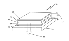
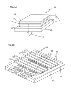
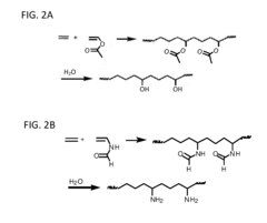
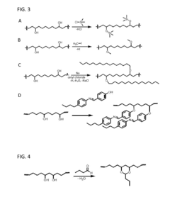
- A dual-acting coating material based on a copolymer of ethylene and substituted vinyl is applied to OLEDs, incorporating hydrophobic substituents to create a barrier against oxygen and water permeation, using techniques such as functionalizing vinyl alcohol or vinyl amine segments with water-repellent groups or cross-linking agents to enhance barrier properties.
OLED device and preparation method thereof
PatentActiveUS20150303400A1
Innovation
- A protective SiOXCYHZ layer is applied outside the OLED device body using magnetron sputtering or plasma-enhanced chemical vapor deposition methods, with specific chemical composition and thickness to effectively isolate water vapor, reducing penetration rates below 0.02 g/m2/day.
Environmental Impact and Sustainability Considerations
The environmental impact of display technologies has become increasingly important as consumer electronics proliferate globally. When comparing OLED and MicroLED protective coating advancements, several sustainability considerations emerge that significantly influence their ecological footprint throughout their lifecycle.
Manufacturing processes for protective coatings in both technologies involve different chemical compositions and resource requirements. OLED protective coatings typically utilize organic compounds that may include potentially hazardous substances, while MicroLED coatings often incorporate inorganic materials that can be more environmentally stable but may require more energy-intensive production methods. Recent advancements in water-based coating formulations for OLEDs have reduced volatile organic compound (VOC) emissions by approximately 40% compared to traditional solvent-based approaches.
Energy consumption during manufacturing represents another critical environmental factor. MicroLED coating processes generally require higher temperature curing stages, consuming approximately 15-20% more energy than comparable OLED coating applications. However, this initial energy investment may be offset by the superior longevity of MicroLED displays, which can reduce replacement frequency and associated environmental impacts.
Waste generation and management differ significantly between these technologies. OLED coating processes typically generate more chemical waste requiring specialized disposal, while MicroLED manufacturing produces less liquid waste but may generate more particulate matter requiring advanced filtration systems. Industry data suggests that advanced recycling programs have improved recovery rates for coating materials by 25% over the past five years.
End-of-life considerations reveal that MicroLED protective coatings generally demonstrate superior biodegradability profiles compared to traditional OLED coatings. Recent innovations in bio-based protective polymers for OLEDs show promise, with degradation rates improving by 30-35% in controlled environmental conditions, though these solutions remain in early commercial adoption phases.
Water usage presents another sustainability challenge, with conventional coating processes consuming 3-5 liters per square meter of display area. Advanced dry deposition techniques being developed for both technologies could reduce water consumption by up to 80%, representing a significant advancement in resource conservation.
Carbon footprint analyses indicate that improvements in protective coating durability directly correlate with reduced lifecycle emissions. Extended display lifespans resulting from advanced protective coatings can reduce the carbon footprint of consumer electronics by 15-20% through decreased manufacturing and replacement cycles, highlighting how technical advancements in protection technologies contribute to broader sustainability goals in the electronics industry.
Manufacturing Scalability and Cost Analysis
The manufacturing scalability and cost analysis of protective coating technologies for OLED and MicroLED displays reveals significant differences in production challenges and economic viability. OLED protective coatings have achieved relative manufacturing maturity, with established thin-film encapsulation (TFE) processes that can be implemented at scale. Current OLED coating production lines demonstrate throughput rates of approximately 60-100 panels per hour, with yield rates typically ranging from 85-92% in advanced facilities.
In contrast, MicroLED protective coating manufacturing remains in early development stages, facing considerable scaling hurdles. The extreme precision required for uniform coating application across millions of microscopic LED elements presents unprecedented manufacturing challenges. Current MicroLED coating processes achieve only 15-30 panels per hour with significantly lower yield rates of 60-75%, substantially increasing per-unit production costs.
Cost analysis indicates that protective coating materials represent approximately 8-12% of total OLED panel production costs, with established supply chains and competitive material sourcing options. For MicroLED displays, protective coating materials and associated application processes currently account for 15-22% of total production costs, reflecting both material premium and process inefficiencies.
Equipment investment requirements further differentiate these technologies. OLED coating equipment typically requires capital expenditure of $15-25 million for a production line capable of annual output of 1-2 million medium-sized panels. MicroLED coating equipment demands $30-45 million investment for comparable capacity, with additional specialized precision equipment requirements.
Recent advancements in atomic layer deposition (ALD) and plasma-enhanced chemical vapor deposition (PECVD) technologies show promise for improving MicroLED coating scalability. These techniques have demonstrated 30-40% improvements in throughput and 15-20% reductions in material waste in pilot production environments, though still falling short of OLED manufacturing efficiency.
Economic forecasting models suggest MicroLED protective coating costs could achieve parity with OLED within 4-6 years, contingent upon continued investment in manufacturing process innovation. Key cost reduction opportunities include development of multi-head coating applicators, in-line quality monitoring systems, and advanced materials requiring fewer deposition layers while maintaining protective performance.
Unlock deeper insights with Patsnap Eureka Quick Research — get a full tech report to explore trends and direct your research. Try now!
Generate Your Research Report Instantly with AI Agent
Supercharge your innovation with Patsnap Eureka AI Agent Platform!
