

Packaging Innovations For High-Power SiC MOSFET Modules
SEP 8, 20259 MIN READ
Generate Your Research Report Instantly with AI Agent
PatSnap Eureka helps you evaluate technical feasibility & market potential.
SiC MOSFET Evolution and Performance Targets
Silicon Carbide (SiC) MOSFET technology has undergone significant evolution since its commercial introduction in the early 2000s. The first-generation devices offered switching speeds and thermal performance superior to silicon counterparts but suffered from reliability issues and high manufacturing costs. By 2010, second-generation SiC MOSFETs emerged with improved gate oxide reliability and reduced on-resistance, marking a critical advancement in the technology's maturity.
The third-generation devices, introduced around 2015, featured optimized cell structures that substantially reduced specific on-resistance while improving short-circuit capability. Current fourth-generation SiC MOSFETs have achieved remarkable performance metrics with RDS(on) values below 2.5 mΩ·cm² for 1200V devices, switching frequencies exceeding 100 kHz, and junction temperatures capable of reaching 200°C under controlled conditions.
Industry roadmaps indicate ambitious performance targets for next-generation SiC MOSFETs. By 2025, the specific on-resistance is expected to approach theoretical limits at approximately 1 mΩ·cm² for 1200V devices, representing a 60% reduction from current commercial offerings. Switching losses are targeted to decrease by 40-50%, enabling power densities exceeding 100 W/cm³ in converter applications.
Temperature performance targets are equally aggressive, with stable operation at junction temperatures of 225-250°C becoming a primary goal. This temperature capability would revolutionize cooling system requirements and enable unprecedented power density in applications like electric vehicle inverters and industrial motor drives.
Reliability metrics are evolving beyond basic parameters to include accelerated lifetime testing under simultaneous thermal, electrical, and mechanical stresses. The industry target is to achieve a failure rate below 1 FIT (failures in time) under standard operating conditions, with projected lifetimes exceeding 20 years in automotive applications.
The scaling trend for SiC MOSFETs shows a consistent pattern of performance improvement, with chip area reduction of approximately 35% per generation while maintaining or improving current handling capability. This scaling trajectory is expected to continue for at least two more generations before fundamental physical limits are encountered.
Performance targets are increasingly application-specific, with automotive-grade SiC MOSFETs focusing on short-circuit withstand time (>10μs) and cosmic ray resilience, while industrial applications prioritize surge current capability and switching performance optimization. This specialization trend reflects the technology's maturation and expanding market penetration across diverse high-power applications.
Market Demand Analysis for High-Power SiC Modules
The global market for Silicon Carbide (SiC) power modules is experiencing unprecedented growth, driven primarily by the rapid expansion of electric vehicles (EVs), renewable energy systems, and industrial power applications. Current market valuations place the SiC power device market at approximately $1.4 billion in 2023, with projections indicating a compound annual growth rate (CAGR) of 34% through 2028, potentially reaching $6 billion.
Electric vehicle applications represent the largest demand segment, accounting for nearly 60% of the total SiC module market. This dominance stems from the critical need for high-efficiency power conversion in EV powertrains, where SiC modules enable longer driving ranges, faster charging capabilities, and reduced cooling requirements compared to traditional silicon-based solutions.
The renewable energy sector constitutes the second-largest market segment at roughly 20%, with particular emphasis on solar inverters and wind power systems. Grid infrastructure modernization projects worldwide are increasingly specifying SiC technology to improve energy transmission efficiency and stability, creating a steady demand growth of 28% annually in this segment.
Industrial applications, including motor drives, uninterruptible power supplies, and factory automation systems, represent approximately 15% of current market demand but are expected to grow at 30% annually as industries pursue energy efficiency improvements and electrification initiatives.
Regionally, Asia-Pacific dominates the market with 45% share, led by China's aggressive investment in electric mobility and renewable energy. North America follows at 30%, with Europe accounting for 20% of global demand. Both regions show accelerated adoption rates driven by stringent emissions regulations and sustainability initiatives.
Customer requirements are evolving rapidly, with particular emphasis on higher power density, improved thermal management, and enhanced reliability. End-users are demanding modules capable of operating at junction temperatures exceeding 200°C while maintaining reliability for 15+ years of operation. This represents a significant challenge for packaging technologies.
Price sensitivity remains a critical factor influencing market penetration. Current SiC module solutions command a 2-3x premium over silicon alternatives, though this gap is narrowing by approximately 10% annually as manufacturing scales increase. Industry analysts predict price parity with silicon IGBT modules in specific power ranges by 2027, which would trigger accelerated adoption across multiple sectors.
The market increasingly demands standardized form factors and pin configurations to facilitate easier system integration and second-sourcing options, creating both challenges and opportunities for packaging innovation that balances customization with interoperability.
Current Packaging Challenges and Thermal Limitations
Silicon Carbide (SiC) MOSFET modules represent a significant advancement in power electronics, offering superior performance compared to traditional silicon-based devices. However, their widespread adoption faces substantial packaging challenges that limit their full potential. The primary obstacle is thermal management - SiC devices can operate at junction temperatures up to 200°C, significantly higher than silicon's typical 150°C limit, creating unprecedented thermal stress on packaging materials and interconnections.
Conventional packaging technologies struggle with the extreme thermal cycling that high-power SiC modules experience. The coefficient of thermal expansion (CTE) mismatch between SiC dies (approximately 4.5 ppm/K) and copper baseplate materials (17 ppm/K) generates severe mechanical stress during operation. This mismatch frequently leads to solder fatigue, delamination, and ultimately device failure, substantially reducing the module's operational lifetime.
Die-attach materials present another critical limitation. Traditional lead-based solders cannot withstand the elevated operating temperatures of SiC devices, while lead-free alternatives often exhibit poorer thermal conductivity and reliability. Silver sintering has emerged as a promising alternative, but implementation challenges related to process control and cost remain significant barriers to widespread adoption.
Wire bonding, the predominant interconnection method, introduces parasitic inductance that restricts switching speed and increases switching losses - negating some of SiC's inherent advantages. Heavy aluminum wire bonds commonly used in power modules are particularly susceptible to fatigue failure under the intense thermal cycling conditions of SiC operation.
Heat dissipation pathways in conventional packages create thermal bottlenecks that prevent SiC devices from operating at their full rated power. The thermal resistance of traditional packaging materials and structures limits heat extraction efficiency, forcing designers to significantly derate SiC devices or implement complex cooling solutions that increase system cost and complexity.
Encapsulation materials used to protect the semiconductor dies and interconnections often degrade under SiC's higher operating temperatures. Conventional silicone gels and epoxy molding compounds may experience accelerated aging, leading to reduced dielectric strength and mechanical protection over time.
Additionally, current packaging approaches struggle with power density limitations. As applications demand increasingly compact solutions, the inability to efficiently extract heat from densely packed SiC dies becomes a critical constraint. This challenge is particularly acute in automotive and industrial applications where space constraints are significant but power requirements continue to increase.
State-of-the-Art Packaging Solutions for SiC MOSFETs
01 Advanced packaging structures for SiC MOSFET modules
Various packaging structures have been developed for SiC MOSFET modules to enhance thermal performance and reliability. These include double-sided cooling designs, direct bonded copper (DBC) substrates, and advanced interconnection technologies. Such packaging structures help to manage the high power density and heat generation of SiC MOSFETs, ensuring optimal performance and extended lifetime of the modules.- Thermal management solutions for SiC MOSFET modules: Silicon Carbide (SiC) MOSFETs generate significant heat during operation, requiring effective thermal management solutions in module packaging. These solutions include advanced heat sink designs, thermal interface materials, and cooling systems that efficiently dissipate heat from the semiconductor devices. Proper thermal management prevents performance degradation and extends the lifespan of SiC MOSFET modules, especially in high-power applications where thermal stress is a critical concern.
- Interconnection techniques for SiC MOSFET modules: Advanced interconnection techniques are essential for SiC MOSFET module packaging to ensure reliable electrical connections while minimizing parasitic inductance and resistance. These techniques include wire bonding, ribbon bonding, silver sintering, and direct copper bonding. The interconnection methods significantly impact the switching performance, power density, and reliability of SiC MOSFET modules, particularly in high-frequency and high-temperature applications where traditional interconnection methods may be inadequate.
- Encapsulation materials and methods for SiC MOSFET modules: Specialized encapsulation materials and methods are crucial for protecting SiC MOSFET modules from environmental factors while maintaining electrical isolation. These include high-temperature silicone gels, epoxy molding compounds, and ceramic-based encapsulants that can withstand the higher operating temperatures of SiC devices. The encapsulation process must address challenges such as coefficient of thermal expansion matching, void prevention, and long-term reliability under thermal cycling conditions.
- Integration of gate drivers and protection circuits in SiC MOSFET modules: Advanced SiC MOSFET module packaging incorporates integrated gate drivers and protection circuits to optimize switching performance and enhance reliability. These integrated solutions address the unique driving requirements of SiC MOSFETs, including faster switching speeds and higher gate voltages. Protection circuits such as overcurrent, overvoltage, and temperature monitoring are integrated within the module package to provide comprehensive device protection while minimizing parasitic effects and improving overall system performance.
- Novel substrate and baseplate materials for SiC MOSFET modules: Innovative substrate and baseplate materials are being developed specifically for SiC MOSFET module packaging to address the higher temperature capabilities of SiC devices. These materials include direct bonded copper (DBC) on aluminum nitride or silicon nitride substrates, active metal brazed (AMB) ceramics, and metal matrix composites for baseplates. The selection of appropriate substrate and baseplate materials is critical for achieving optimal thermal performance, mechanical stability, and reliability in high-temperature and high-power applications.
02 Thermal management solutions in SiC MOSFET packaging
Effective thermal management is critical in SiC MOSFET module packaging due to the high operating temperatures of these devices. Solutions include integrated cooling systems, advanced thermal interface materials, and optimized heat sink designs. These thermal management approaches help to dissipate heat efficiently, prevent thermal runaway, and maintain the electrical performance of SiC MOSFET modules under high-power conditions.Expand Specific Solutions03 Interconnection technologies for SiC MOSFET modules
Innovative interconnection technologies are employed in SiC MOSFET module packaging to minimize parasitic inductance and resistance. These include silver sintering, copper wire bonding, and clip bonding techniques. Advanced interconnection methods improve the electrical performance, switching speed, and reliability of SiC MOSFET modules while enabling higher power density and efficiency.Expand Specific Solutions04 Encapsulation and protection methods for SiC MOSFET modules
Various encapsulation and protection methods are used in SiC MOSFET module packaging to shield the devices from environmental factors and mechanical stress. These include silicone gel encapsulation, molding compounds, and hermetic sealing techniques. Proper encapsulation ensures long-term reliability, prevents moisture ingress, and protects against thermal cycling and vibration in harsh operating environments.Expand Specific Solutions05 Integration of gate drivers and protection circuits in SiC MOSFET modules
Advanced SiC MOSFET module packaging incorporates integrated gate drivers and protection circuits to optimize switching performance and enhance reliability. These integrated solutions include overcurrent protection, short-circuit protection, and temperature monitoring features. The close integration of driving and protection circuits minimizes parasitic elements, improves switching characteristics, and provides comprehensive protection for the SiC MOSFET devices.Expand Specific Solutions
Leading Manufacturers and Competitive Landscape
The SiC MOSFET module packaging innovation market is currently in a growth phase, with increasing adoption driven by electric vehicle and renewable energy applications. The global market is projected to expand significantly as SiC technology matures, offering superior performance over traditional silicon-based solutions. Leading semiconductor manufacturers like Wolfspeed, Infineon, TSMC, and Fuji Electric are competing with emerging players such as Yangjie Electronic and CRRC Times Semiconductor. Academic institutions including Xi'an Jiaotong University and Zhejiang University are contributing significant research. The technology is advancing from early adoption to mainstream implementation, with innovations focusing on thermal management, reliability, and power density improvements to address high-power application demands.
Taiwan Semiconductor Manufacturing Co., Ltd.
Technical Solution: TSMC has developed advanced packaging solutions for SiC power modules leveraging their expertise in semiconductor manufacturing and advanced packaging technologies. Their approach incorporates innovative copper clip bonding technology that replaces traditional aluminum wire bonds, reducing package resistance by approximately 40% and package inductance by up to 60%. TSMC's SiC module packaging implements a proprietary sintered silver die-attach process that provides superior thermal performance with thermal conductivity exceeding 200 W/m·K, significantly higher than conventional solder materials. Their packaging technology features advanced DBC substrates with optimized layout and integrated cooling structures that achieve junction-to-case thermal resistance below 0.15°C/W for high-power modules. TSMC has also pioneered the implementation of wafer-level packaging techniques for SiC devices, enabling smaller form factors and improved thermal performance through elimination of traditional wire bonds and implementation of through-silicon vias (TSVs) for vertical current flow.
Strengths: Industry-leading manufacturing precision and quality control; advanced copper clip technology significantly reduces parasitic inductance; superior thermal management through innovative materials and structures. Weaknesses: Relatively new entrant to SiC power module market compared to established power semiconductor companies; limited product portfolio breadth; higher cost structure for specialized packaging solutions.
Infineon Technologies Americas Corp.
Technical Solution: Infineon has developed the CoolSiC™ module family featuring innovative packaging technologies specifically optimized for SiC MOSFETs. Their modules implement a baseplate-free design with direct liquid cooling capability, reducing thermal resistance by up to 40% compared to conventional modules. Infineon's packaging technology incorporates pre-applied TIM (Thermal Interface Material) and PressFIT connection technology that eliminates the need for soldering, improving reliability and simplifying assembly. Their EasyPACK™ modules feature an integrated NTC temperature sensor and an advanced internal layout that minimizes parasitic inductance to approximately 8 nH. Infineon has also pioneered the implementation of .XT connection technology in SiC modules, which uses diffusion soldering and copper wire bonding to achieve power cycling capability 10 times higher than standard technologies, enabling reliable operation at junction temperatures up to 175°C.
Strengths: Comprehensive module portfolio covering various power ranges; advanced .XT interconnection technology significantly improves reliability; baseplate-free designs reduce thermal resistance and weight. Weaknesses: Higher initial cost compared to silicon solutions; some designs still rely on aluminum wire bonding which limits maximum operating temperature; thermal cycling performance still presents challenges in automotive applications.
Key Patents in High-Temperature SiC Module Packaging
High power silicon carbide and silicon semiconductor device package
PatentInactiveUS20040130021A1
Innovation
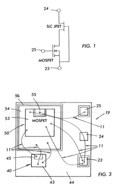
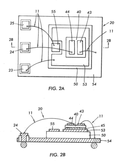
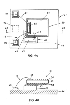
- A hybrid transistor structure is created by co-packaging a silicon carbide field effect transistor (SiCFET) with a silicon MOSFET in a die-on-die configuration, where the SiCFET is mounted electrode-on-electrode with the MOSFET, allowing for shared thermal management and reduced footprint, with the SiCFET providing faster switching and improved thermal management through shared heat sinks.

Silicon carbide semiconductor device
PatentPendingUS20240234569A9
Innovation
- A silicon carbide semiconductor device with a hybrid gate structure featuring a trench gate configuration that reduces JFET resistance and parasitic gate-to-drain capacitance, enhancing switching performance by increasing channel width density and optimizing the layout of doped regions and trenches.
Reliability Testing Standards for SiC Power Modules
Reliability testing standards for SiC power modules have evolved significantly to address the unique characteristics and failure mechanisms of silicon carbide technology. These standards are crucial for ensuring the long-term performance and safety of high-power SiC MOSFET modules in demanding applications such as electric vehicles, renewable energy systems, and industrial drives.
The Joint Electron Device Engineering Council (JEDEC) has established specific qualification standards for wide bandgap semiconductors, including JEP180 and JEP173, which outline testing methodologies tailored to SiC devices. These standards incorporate enhanced temperature cycling tests that reflect the higher operating temperatures of SiC modules (typically up to 200°C) compared to traditional silicon-based modules.
Power cycling tests have been modified to account for SiC's unique thermal behavior, with standards now requiring more aggressive ΔT conditions and higher maximum temperatures. The IEC 60749 series has been adapted with specific provisions for SiC technology, particularly addressing the bond wire fatigue and solder degradation that occur under the higher thermal stress conditions typical of SiC operation.
Short-circuit robustness testing has gained prominence in SiC reliability standards due to the material's reduced short-circuit withstand time compared to silicon. Standards now specify more stringent short-circuit survival requirements, typically demanding withstand capabilities of at least 5-10 μs at rated voltage and current conditions.
Humidity and bias testing protocols have been intensified to address SiC's susceptibility to threshold voltage shifts under gate bias and humidity conditions. The HTRB (High Temperature Reverse Bias) and H3TRB (High Humidity High Temperature Reverse Bias) tests now commonly specify extended durations of 1000+ hours for SiC modules.
Dielectric testing standards have evolved to accommodate the higher electric field strengths in SiC devices, with partial discharge testing becoming a standard requirement due to the higher blocking voltages (commonly 1200V to 3300V) in SiC modules. The IEC 61287 standard has been updated to include specific provisions for measuring and qualifying partial discharge in SiC power modules.
Automotive-grade qualification standards such as AQG 324 and AEC-Q101 have incorporated SiC-specific test conditions, recognizing the growing adoption of SiC technology in electric vehicle powertrains. These standards mandate more rigorous vibration and mechanical shock testing to ensure reliability in automotive environments.
Environmental Impact of Advanced SiC Packaging Materials
The environmental impact of SiC MOSFET packaging materials represents a critical consideration in the sustainable development of power electronics. Advanced SiC packaging solutions, while offering superior thermal and electrical performance, introduce complex environmental trade-offs throughout their lifecycle. The materials commonly used in high-power SiC MOSFET modules—including copper, aluminum, ceramics, and various polymers—each carry distinct environmental footprints related to resource extraction, manufacturing processes, and end-of-life management.
Manufacturing processes for advanced SiC packaging materials typically require significant energy inputs and may involve hazardous chemicals. For instance, the production of high-purity ceramics like aluminum nitride (AlN) and silicon nitride (Si3N4) demands high-temperature processing that contributes to greenhouse gas emissions. Similarly, the metallization processes used for creating interconnects often involve electroplating techniques that generate wastewater containing heavy metals and other contaminants.
Life cycle assessment (LCA) studies indicate that the environmental benefits of SiC technology during operation—primarily energy savings due to higher efficiency—may outweigh the environmental costs of production. A typical high-power SiC MOSFET module can reduce energy consumption by 20-30% compared to silicon alternatives, potentially offsetting initial manufacturing impacts within 1-3 years of operation depending on application frequency and load conditions.
Recent innovations in SiC packaging are increasingly focused on environmental sustainability. Lead-free solders are replacing traditional tin-lead alloys, addressing concerns about heavy metal contamination. Additionally, research into bio-based polymers for encapsulation materials shows promise for reducing petroleum dependency in packaging components. These materials demonstrate comparable thermal stability while offering improved biodegradability at end-of-life.
Recyclability presents another significant challenge for SiC module packaging. The multi-material nature of these packages—combining metals, ceramics, and polymers in complex arrangements—complicates separation and recovery processes. Emerging design-for-disassembly approaches aim to facilitate material recovery, with some manufacturers implementing modular designs that allow for easier separation of components at end-of-life.
Water usage in manufacturing processes for advanced packaging materials also warrants attention. Semiconductor packaging typically requires ultrapure water for cleaning processes, with a single facility potentially consuming millions of gallons annually. Water recycling systems and dry cleaning technologies are being developed to mitigate this impact, with some facilities reporting water reuse rates exceeding 80%.
The transition to more environmentally friendly packaging materials must balance performance requirements with sustainability goals. As regulatory frameworks like the European Union's Restriction of Hazardous Substances (RoHS) and Waste Electrical and Electronic Equipment (WEEE) directives become more stringent, manufacturers are increasingly incentivized to develop packaging solutions that minimize environmental impact while maintaining the thermal and electrical performance necessary for high-power SiC MOSFET applications.
Unlock deeper insights with PatSnap Eureka Quick Research — get a full tech report to explore trends and direct your research. Try now!
Generate Your Research Report Instantly with AI Agent
Supercharge your innovation with PatSnap Eureka AI Agent Platform!