Performance Metrics For Evaluating SiC MOSFET Efficiency
SEP 8, 202510 MIN READ
Generate Your Research Report Instantly with AI Agent
Patsnap Eureka helps you evaluate technical feasibility & market potential.
SiC MOSFET Technology Evolution and Efficiency Goals
Silicon Carbide (SiC) MOSFET technology has undergone significant evolution since its initial development in the early 1990s. The journey began with rudimentary devices exhibiting high on-resistance and limited switching capabilities, primarily confined to laboratory environments. By the early 2000s, commercial viability emerged as manufacturers like Cree (now Wolfspeed) and Rohm introduced first-generation SiC MOSFETs with blocking voltages of 1200V, marking a crucial milestone in power electronics.
The technology evolution accelerated between 2010-2015 with second-generation devices featuring improved channel mobility and reduced on-resistance, decreasing from initial values of 20 mΩ·cm² to approximately 3-4 mΩ·cm². This period also witnessed enhanced gate oxide reliability and stability, addressing early concerns about oxide breakdown under high electric fields characteristic of wide bandgap semiconductors.
From 2015 onwards, third-generation SiC MOSFETs emerged with optimized cell structures, trench gate designs, and refined manufacturing processes that significantly reduced defect densities. These advancements enabled higher current densities and improved thermal performance, expanding application possibilities beyond initial niche markets into mainstream power conversion systems.
The efficiency goals for SiC MOSFETs have evolved in parallel with technological capabilities. Initial targets focused on achieving basic functionality at high voltages (>1000V) while maintaining reasonable switching losses. As the technology matured, efficiency goals shifted toward reducing specific on-resistance (RDS(on)) below 2 mΩ·cm² while simultaneously improving switching performance to enable operation at frequencies exceeding 100 kHz with minimal losses.
Current efficiency targets center on achieving ultra-low switching losses (<10 μJ) at high frequencies (>200 kHz) while maintaining excellent conduction performance. This combination enables overall system efficiency improvements of 2-3% compared to silicon-based solutions, which translates to significant energy savings in high-power applications such as electric vehicle inverters and renewable energy systems.
Future evolution paths aim at pushing specific on-resistance below 1 mΩ·cm² while enhancing reliability metrics such as gate oxide lifetime beyond 20 years under typical operating conditions. Additional efficiency goals include reducing temperature dependence of key parameters and improving short-circuit withstand capability to enhance robustness in demanding applications.
The industry roadmap projects continued refinement of SiC MOSFET technology with particular emphasis on cost reduction through larger wafer sizes (transitioning from current 150mm to 200mm and eventually 300mm), improved manufacturing yields, and simplified packaging solutions that optimize thermal performance while reducing parasitic inductances that limit high-frequency operation.
Market Demand Analysis for High-Efficiency Power Semiconductors
The global power semiconductor market is experiencing unprecedented growth, driven primarily by the increasing demand for energy-efficient solutions across multiple industries. Silicon Carbide (SiC) MOSFETs, as next-generation power semiconductors, are positioned at the forefront of this market transformation. Current market valuations place the SiC power device market at approximately $1.1 billion in 2023, with projections indicating a compound annual growth rate (CAGR) of 34% through 2028.
Electric vehicle (EV) manufacturing represents the largest and fastest-growing segment for SiC MOSFET applications. With automotive manufacturers committing to electrification targets, the demand for high-efficiency power semiconductors that can operate at higher voltages, temperatures, and switching frequencies continues to surge. Industry reports indicate that a single electric vehicle can contain SiC components worth $500-$1,000, representing a substantial market opportunity as EV production scales globally.
Industrial power supplies constitute another significant market segment, where efficiency improvements directly translate to operational cost savings. The industrial sector's transition toward more energy-efficient systems has created a demand for SiC MOSFETs that can deliver efficiency improvements of 20-30% compared to traditional silicon-based alternatives. This efficiency gain becomes particularly valuable in high-power applications where energy losses translate to substantial operational costs.
Renewable energy systems, particularly solar inverters and wind power converters, represent a rapidly expanding application area for SiC MOSFETs. The market for SiC in renewable energy applications is growing at approximately 40% annually, driven by the global push toward sustainable energy sources and the need for more efficient power conversion systems. Higher efficiency in these applications directly correlates with increased energy harvest and improved return on investment for renewable energy projects.
Data center power infrastructure presents another high-growth market segment, with efficiency becoming increasingly critical as data centers expand globally. The power density advantages of SiC MOSFETs allow for smaller form factors and reduced cooling requirements, addressing key challenges in modern data center design. Industry analysts estimate that SiC-based power systems can reduce data center energy consumption by 15-20%, representing significant operational savings.
Market research indicates that customers across these segments are increasingly prioritizing total cost of ownership over initial acquisition costs, creating favorable conditions for premium-priced SiC solutions that deliver superior performance metrics. This shift in purchasing behavior is accelerating SiC MOSFET adoption despite their current price premium of 2-3 times compared to silicon alternatives.
Current SiC MOSFET Performance Benchmarks and Limitations
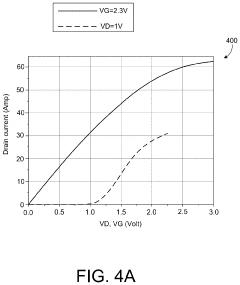
Silicon Carbide (SiC) MOSFETs have emerged as superior alternatives to traditional silicon-based power devices, particularly in high-power and high-frequency applications. Current performance benchmarks for SiC MOSFETs demonstrate significant advantages in several key metrics compared to their silicon counterparts. The on-resistance (RDS(on)) of commercial SiC MOSFETs typically ranges from 10 to 100 mΩ, representing a 5-10x improvement over silicon devices with equivalent voltage ratings. This lower on-resistance directly translates to reduced conduction losses, which can account for 30-50% of total power losses in switching applications.
Switching performance metrics show that SiC MOSFETs can operate efficiently at frequencies exceeding 100 kHz, with some specialized designs reaching 500 kHz or higher. The switching energy losses (Eon and Eoff) are typically 3-5 times lower than comparable silicon IGBTs, enabling higher frequency operation without excessive thermal penalties. Turn-on and turn-off times are in the range of 10-30 nanoseconds, significantly faster than silicon alternatives.
Thermal performance represents another critical benchmark area. Current SiC MOSFETs demonstrate junction-to-case thermal resistance (Rth(j-c)) values between 0.3 and 0.7 °C/W, allowing them to operate reliably at junction temperatures up to 175-200°C, compared to the 150°C limit of silicon devices. This superior thermal capability enables higher power density designs and reduces cooling requirements.
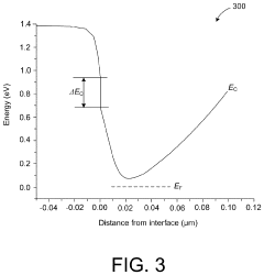
Despite these impressive benchmarks, SiC MOSFETs face several limitations. Gate oxide reliability remains a significant concern, with current devices showing higher defect densities at the SiC/SiO2 interface compared to silicon. This results in threshold voltage instability and potential long-term reliability issues, particularly under high-temperature operation. Commercial devices typically show threshold voltage shifts of 0.1-0.5V after extended high-temperature operation.
Channel mobility in SiC MOSFETs remains substantially lower than theoretical predictions, typically achieving only 20-40 cm²/V·s compared to potential values exceeding 100 cm²/V·s. This limitation directly impacts on-resistance and overall efficiency. The cause is primarily attributed to interface traps and channel defects that have not been fully mitigated in current manufacturing processes.
Cost remains a significant limitation, with SiC MOSFETs typically priced 3-5 times higher than silicon alternatives with similar ratings. This price premium, while decreasing annually by approximately 10-15%, still presents a barrier to widespread adoption in cost-sensitive applications. Manufacturing yields for SiC devices hover around 70-85%, compared to >95% for mature silicon processes, contributing significantly to this cost differential.
Package-related limitations also impact performance, as traditional packaging technologies struggle to fully leverage SiC's high-temperature and high-frequency capabilities. Parasitic inductances in standard packages (typically 5-15 nH) can negate some of SiC's inherent switching speed advantages, necessitating advanced packaging solutions that are still evolving.
Switching performance metrics show that SiC MOSFETs can operate efficiently at frequencies exceeding 100 kHz, with some specialized designs reaching 500 kHz or higher. The switching energy losses (Eon and Eoff) are typically 3-5 times lower than comparable silicon IGBTs, enabling higher frequency operation without excessive thermal penalties. Turn-on and turn-off times are in the range of 10-30 nanoseconds, significantly faster than silicon alternatives.
Thermal performance represents another critical benchmark area. Current SiC MOSFETs demonstrate junction-to-case thermal resistance (Rth(j-c)) values between 0.3 and 0.7 °C/W, allowing them to operate reliably at junction temperatures up to 175-200°C, compared to the 150°C limit of silicon devices. This superior thermal capability enables higher power density designs and reduces cooling requirements.
Despite these impressive benchmarks, SiC MOSFETs face several limitations. Gate oxide reliability remains a significant concern, with current devices showing higher defect densities at the SiC/SiO2 interface compared to silicon. This results in threshold voltage instability and potential long-term reliability issues, particularly under high-temperature operation. Commercial devices typically show threshold voltage shifts of 0.1-0.5V after extended high-temperature operation.
Channel mobility in SiC MOSFETs remains substantially lower than theoretical predictions, typically achieving only 20-40 cm²/V·s compared to potential values exceeding 100 cm²/V·s. This limitation directly impacts on-resistance and overall efficiency. The cause is primarily attributed to interface traps and channel defects that have not been fully mitigated in current manufacturing processes.
Cost remains a significant limitation, with SiC MOSFETs typically priced 3-5 times higher than silicon alternatives with similar ratings. This price premium, while decreasing annually by approximately 10-15%, still presents a barrier to widespread adoption in cost-sensitive applications. Manufacturing yields for SiC devices hover around 70-85%, compared to >95% for mature silicon processes, contributing significantly to this cost differential.
Package-related limitations also impact performance, as traditional packaging technologies struggle to fully leverage SiC's high-temperature and high-frequency capabilities. Parasitic inductances in standard packages (typically 5-15 nH) can negate some of SiC's inherent switching speed advantages, necessitating advanced packaging solutions that are still evolving.
Established Methodologies for SiC MOSFET Performance Evaluation
01 SiC MOSFET device structure optimization
Silicon Carbide (SiC) MOSFET efficiency can be improved through structural optimizations of the device. These optimizations include enhanced gate designs, improved channel mobility, optimized drift region structures, and reduced parasitic capacitances. By refining the device architecture, manufacturers can achieve lower on-resistance, faster switching speeds, and reduced conduction losses, all contributing to higher overall efficiency in power conversion applications.- SiC MOSFET device structure optimization: Silicon Carbide (SiC) MOSFET efficiency can be significantly improved through structural optimizations of the device. These optimizations include refining the gate structure, enhancing the channel mobility, reducing parasitic capacitances, and improving the interface quality between SiC and gate dielectric. Advanced fabrication techniques like trench gate structures and double-implanted MOSFETs help minimize on-resistance while maintaining high breakdown voltage capabilities, directly contributing to higher power conversion efficiency.
- Power conversion circuit design with SiC MOSFETs: Efficiency improvements in SiC MOSFET applications heavily depend on optimized power conversion circuit designs. These designs incorporate specialized gate driving techniques, switching frequency optimization, and thermal management solutions tailored specifically for SiC devices. Advanced topologies like soft-switching circuits, resonant converters, and multilevel inverters leverage SiC MOSFETs' fast switching capabilities while minimizing switching losses. Proper circuit layout and component selection further enhance overall system efficiency by reducing parasitic inductances and resistances.
- Thermal management and packaging solutions: Effective thermal management is crucial for maximizing SiC MOSFET efficiency. Advanced packaging technologies with improved thermal conductivity materials help dissipate heat more efficiently, allowing SiC devices to operate at higher power densities without performance degradation. Innovative cooling solutions including direct liquid cooling, double-sided cooling, and advanced thermal interface materials significantly reduce junction temperatures. Lower operating temperatures directly translate to reduced conduction losses and improved long-term reliability, ultimately enhancing overall system efficiency.
- Gate driver optimization for SiC MOSFETs: Specialized gate driver designs are essential for fully exploiting SiC MOSFETs' efficiency potential. These drivers feature optimized gate voltage levels, precise timing control, and appropriate slew rate management to balance switching speed with electromagnetic interference. Advanced gate driver solutions incorporate active Miller clamping, desaturation protection, and temperature compensation to maintain optimal performance across operating conditions. Intelligent gate driving techniques that adapt to changing load conditions further minimize switching losses while ensuring reliable operation.
- System-level integration and control strategies: System-level integration approaches focus on holistic efficiency improvements by optimizing the interaction between SiC MOSFETs and other system components. Advanced control algorithms specifically designed for SiC-based power converters implement precise switching timing, dead-time optimization, and adaptive modulation techniques. These strategies often incorporate real-time monitoring and dynamic adjustment capabilities to maintain peak efficiency across varying operating conditions. Integration with digital control systems enables sophisticated power management features that further enhance overall system performance and energy utilization.
02 Advanced driving and control techniques
Implementing sophisticated driving and control techniques can significantly enhance SiC MOSFET efficiency. These techniques include optimized gate driving circuits, advanced pulse width modulation strategies, and intelligent control algorithms that minimize switching losses. Proper gate voltage control, timing optimization, and driver impedance matching help to fully leverage the inherent advantages of SiC technology, resulting in improved thermal performance and higher efficiency in power conversion systems.Expand Specific Solutions03 Thermal management solutions
Effective thermal management is crucial for maximizing SiC MOSFET efficiency. Various cooling techniques and packaging innovations help to dissipate heat more efficiently, allowing the devices to operate at lower temperatures. These solutions include advanced heat sink designs, improved thermal interface materials, and innovative packaging technologies that reduce thermal resistance. By maintaining lower operating temperatures, SiC MOSFETs can achieve higher current densities and improved reliability while maintaining optimal efficiency.Expand Specific Solutions04 Power converter topology optimization
Optimizing power converter topologies specifically for SiC MOSFETs can significantly improve system efficiency. These optimizations include resonant and soft-switching circuits that reduce switching losses, multilevel converter designs that distribute stress more evenly, and innovative circuit configurations that minimize parasitic effects. By designing converter topologies that leverage the unique characteristics of SiC devices, engineers can achieve higher switching frequencies, reduced filtering requirements, and improved overall system efficiency.Expand Specific Solutions05 Material quality and fabrication improvements
Advancements in SiC material quality and fabrication processes directly impact MOSFET efficiency. Improvements include higher purity substrate materials, enhanced epitaxial growth techniques, optimized doping profiles, and refined interface treatments. These advancements reduce defect densities at the semiconductor-oxide interface, improve channel mobility, and enhance overall device performance. By continually refining material quality and manufacturing processes, SiC MOSFETs can achieve lower losses and higher efficiency in power conversion applications.Expand Specific Solutions
Key Industry Players in SiC MOSFET Manufacturing
The SiC MOSFET efficiency evaluation landscape is currently in a growth phase, with the market expanding rapidly due to increasing demand for high-efficiency power electronics. Academic institutions like University of Electronic Science & Technology of China, Chongqing University, and North China Electric Power University are leading research efforts, while companies including Infineon Technologies, Huawei, and State Grid are driving commercial applications. The technology has reached moderate maturity with standardized performance metrics emerging, though optimization continues. Key players are focusing on improving thermal performance, switching characteristics, and reliability parameters, with collaboration between academia and industry accelerating development of more sophisticated evaluation frameworks for next-generation SiC MOSFET technologies.
University of Electronic Science & Technology of China
Technical Solution: UESTC has developed a comprehensive SiC MOSFET evaluation framework focusing on both static and dynamic performance metrics. Their approach includes advanced characterization of temperature-dependent on-resistance (RDS(on)) across a wide operating range (-55°C to 200°C), revealing the unique positive temperature coefficient behavior that enables reliable parallel operation. Their research team has pioneered high-precision switching loss measurement techniques using custom-designed double-pulse test setups with coaxial current shunts achieving bandwidth exceeding 100MHz for accurate high-speed switching characterization. UESTC's methodology incorporates detailed analysis of gate oxide reliability metrics, including threshold voltage stability under repetitive switching and bias temperature stress testing protocols. They've developed novel figure-of-merit calculations combining RDS(on) × Qg (gate charge) and RDS(on) × Eoss (output capacitance energy) to provide comprehensive efficiency comparisons between different device technologies. Their evaluation system also includes specialized short-circuit withstand time measurements and analysis of body diode reverse recovery characteristics, which significantly impact overall system efficiency in many applications.
Strengths: Exceptionally rigorous academic approach with comprehensive measurement methodologies that provide deep insights into fundamental device physics and performance limitations. Their evaluation techniques are well-documented in academic literature, making them accessible to the broader research community. Weaknesses: Their evaluation framework sometimes emphasizes theoretical performance limits over practical application considerations in real-world power conversion systems.
Infineon Technologies AG
Technical Solution: Infineon has developed comprehensive performance evaluation frameworks for SiC MOSFETs that focus on multiple efficiency metrics. Their approach includes dynamic characterization methods measuring switching energy losses (Eon, Eoff) across various operating temperatures (-40°C to 175°C) and current levels. They've pioneered advanced gate driver optimization techniques specifically for SiC devices, achieving switching loss reductions of up to 30% compared to conventional drivers. Infineon's evaluation methodology incorporates thermal performance metrics including junction-to-case thermal resistance (Rth(j-c)) measurements and transient thermal impedance characterization to accurately predict device behavior under real-world conditions. Their benchmarking system evaluates SiC MOSFETs against silicon IGBTs in identical power conversion topologies, demonstrating efficiency improvements of 2-3% at system level, which translates to significant energy savings in high-power applications. Infineon also employs accelerated lifetime testing protocols to correlate performance metrics with long-term reliability, including gate oxide stability testing and body diode degradation analysis.
Strengths: Industry-leading comprehensive evaluation framework that balances switching performance with thermal management and reliability metrics. Their approach provides holistic efficiency assessment rather than focusing on single parameters. Weaknesses: Their evaluation methods often require sophisticated testing equipment not accessible to smaller manufacturers, and some proprietary metrics make direct comparison with competitors' devices challenging.
Critical Parameters and Testing Standards for SiC MOSFETs
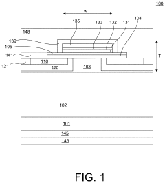
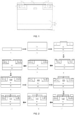
Silicon carbide field-effect transistors
PatentActiveUS20220013661A1
Innovation
- A silicon carbide (SiC) metal-oxide-semiconductor field-effect transistor (MOSFET) design incorporating a substrate, drift region, spreading layer, body region, and source region with a gate structure that includes a gate oxide layer, aluminum nitride, and p-type gallium nitride layers, achieving low on-state specific resistance and high threshold voltage.
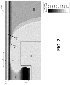
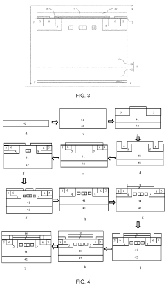
Silicon carbide metal oxide semiconductor field effect transistor and manufacturing method therefor
PatentInactiveEP3813127A1
Innovation
- A silicon carbide metal-oxide-semiconductor field-effect transistor structure is developed, incorporating a second conduction type epitaxial layer, first conduction type well regions, and additional doping regions within the JFET region to reduce gate oxide electric field strength, including a gate oxide layer and passivation protection, with specific doping concentrations and geometries to enhance device performance.
Thermal Management Considerations for SiC MOSFET Applications
Thermal management is a critical aspect of SiC MOSFET applications that directly impacts device efficiency and reliability. Silicon Carbide MOSFETs operate at significantly higher temperatures than traditional silicon devices, with junction temperatures capable of reaching up to 200°C compared to silicon's typical 150°C limit. This extended temperature range offers performance advantages but introduces unique thermal management challenges that must be addressed to fully realize SiC MOSFET efficiency benefits.
The superior thermal conductivity of SiC material (approximately 3-4 times that of silicon) provides an inherent advantage in heat dissipation. However, the higher power density capabilities of SiC MOSFETs often result in more concentrated heat generation that requires sophisticated cooling solutions. Effective thermal management strategies must consider both static and dynamic thermal behaviors, as transient thermal impedance becomes increasingly important in high-frequency switching applications.
Heat spreading techniques play a vital role in SiC MOSFET thermal management. Advanced packaging technologies such as direct bonded copper (DBC) substrates and silver sintering die-attach materials have demonstrated 30-40% improvement in thermal resistance compared to conventional soldering methods. These technologies enhance heat transfer from the die to the heatsink, reducing thermal resistance and allowing for higher operational power densities.
Cooling system design for SiC MOSFETs requires careful consideration of thermal interface materials (TIMs) and heatsink configurations. Studies indicate that the thermal resistance of the TIM layer can account for up to 30% of the total junction-to-ambient thermal resistance. Advanced TIMs with higher thermal conductivity, such as metal-based composites or phase change materials, can significantly reduce this bottleneck in the thermal path.
Active cooling solutions, including forced air and liquid cooling systems, become increasingly necessary as power densities rise. Liquid cooling systems have demonstrated the ability to handle heat fluxes exceeding 500 W/cm², making them particularly suitable for high-power SiC applications. The implementation of two-phase cooling technologies, such as jet impingement or microchannel coolers, can further enhance cooling efficiency by leveraging the latent heat of vaporization.
Temperature monitoring and thermal protection strategies are essential components of SiC MOSFET thermal management. Integrated temperature sensors and advanced thermal modeling techniques enable real-time monitoring and protection against thermal runaway conditions. Sophisticated thermal models that account for the unique properties of SiC materials allow for more accurate prediction of temperature distributions and hotspots within the device structure.
The relationship between thermal management and overall system efficiency is particularly pronounced in SiC applications. Effective thermal solutions not only prevent device failure but also optimize performance by maintaining operation within ideal temperature ranges. Research indicates that for every 10°C reduction in junction temperature, SiC MOSFET lifetime can potentially double, highlighting the critical importance of thermal management in ensuring long-term reliability and maximizing return on investment in SiC technology.
Sustainability and Environmental Impact of SiC Technology
Silicon Carbide (SiC) technology represents a significant advancement in power electronics with substantial environmental benefits compared to traditional silicon-based devices. The superior efficiency of SiC MOSFETs directly translates to reduced energy consumption across various applications, contributing to lower greenhouse gas emissions. When evaluating the sustainability impact of SiC technology, lifecycle assessment studies indicate that despite the higher energy requirements during manufacturing, the operational efficiency gains over device lifetime result in net positive environmental outcomes.
The reduced switching and conduction losses in SiC MOSFETs enable more compact power conversion systems that require fewer passive components and smaller cooling solutions. This material efficiency translates to reduced resource consumption and smaller physical footprints for power electronics systems. Additionally, the higher temperature tolerance of SiC devices allows for simplified cooling requirements, further reducing the environmental impact associated with thermal management systems.
SiC technology plays a pivotal role in enabling renewable energy integration by improving the efficiency of power conversion in solar inverters, wind power systems, and energy storage solutions. The higher switching frequencies possible with SiC MOSFETs allow for more efficient energy harvesting and conversion, directly supporting the transition to renewable energy sources. Performance metrics for SiC MOSFETs must therefore include not only electrical efficiency parameters but also metrics related to their contribution to overall system sustainability.
The extended operational lifetime of SiC devices—often exceeding 15-20 years compared to 8-10 years for silicon alternatives—significantly reduces electronic waste generation. This longevity, combined with the potential for recycling SiC materials, presents opportunities for circular economy approaches in the semiconductor industry. However, challenges remain in establishing cost-effective recycling processes for end-of-life SiC devices.
From a regulatory perspective, SiC technology aligns well with global energy efficiency standards and carbon reduction initiatives. The adoption of SiC MOSFETs in electric vehicles, industrial drives, and grid infrastructure directly supports policy objectives for energy conservation and emissions reduction. As performance metrics evolve, they increasingly incorporate sustainability indicators such as carbon footprint per kilowatt processed, embodied energy payback periods, and contribution to system-level efficiency improvements.
Looking forward, the environmental benefits of SiC technology will likely expand as manufacturing processes mature and economies of scale reduce production energy intensity. Research into more sustainable manufacturing techniques and material sourcing for SiC devices represents an important frontier for further enhancing the environmental credentials of this promising technology.
Unlock deeper insights with Patsnap Eureka Quick Research — get a full tech report to explore trends and direct your research. Try now!
Generate Your Research Report Instantly with AI Agent
Supercharge your innovation with Patsnap Eureka AI Agent Platform!