Regulatory Frameworks for Silicon Carbide Wafer Production
OCT 14, 20259 MIN READ
Generate Your Research Report Instantly with AI Agent
Patsnap Eureka helps you evaluate technical feasibility & market potential.
SiC Wafer Technology Background and Objectives
Silicon Carbide (SiC) wafer technology has evolved significantly since its initial development in the early 20th century. The journey began with the Acheson process for SiC powder production in 1892, followed by the Lely method for crystal growth in 1955. However, it wasn't until the 1980s that serious commercial interest in SiC wafers emerged, driven by their exceptional properties for power electronics applications.
The technological evolution of SiC wafers has been marked by continuous improvements in crystal growth techniques, particularly the physical vapor transport (PVT) method, which remains the industry standard. Over the past decade, significant advancements have been made in reducing defect densities, increasing wafer diameters, and improving surface quality, enabling the transition from primarily research applications to commercial production.
Current SiC wafer technology offers remarkable advantages over traditional silicon, including a wider bandgap (3.2 eV compared to 1.1 eV for silicon), higher breakdown electric field strength (approximately 10 times that of silicon), and superior thermal conductivity (3-4 times higher than silicon). These properties make SiC ideal for high-power, high-temperature, and high-frequency applications.
The regulatory landscape for SiC wafer production has evolved in response to industry growth, with frameworks addressing manufacturing standards, quality control parameters, and environmental considerations. Early regulations focused primarily on worker safety due to the abrasive nature of SiC materials, but have expanded to encompass comprehensive manufacturing guidelines as the industry has matured.
The primary objective of current regulatory frameworks is to establish standardized production protocols that ensure consistent wafer quality while minimizing environmental impact. This includes specifications for crystal growth parameters, defect characterization methodologies, and wafer finishing processes. Additionally, regulations aim to address the energy-intensive nature of SiC production by promoting more efficient manufacturing techniques.
Looking forward, the technological trajectory suggests continued improvements in wafer diameter (moving beyond current 150mm standards to 200mm and eventually 300mm), defect reduction (particularly basal plane dislocations and micropipes), and cost efficiency. Regulatory frameworks will need to evolve accordingly, with particular emphasis on sustainability metrics as production volumes increase to meet growing demand from electric vehicle, renewable energy, and industrial sectors.
The convergence of technological advancement and regulatory development in SiC wafer production represents a critical foundation for the next generation of power electronics, with implications spanning multiple industries and global energy efficiency initiatives.
Market Analysis for SiC Wafer Applications
The silicon carbide (SiC) wafer market has experienced remarkable growth in recent years, driven primarily by increasing demand in power electronics, electric vehicles, and renewable energy applications. The global SiC wafer market was valued at approximately $420 million in 2020 and is projected to reach $1.5 billion by 2027, representing a compound annual growth rate of nearly 20%. This substantial growth trajectory underscores the critical importance of SiC wafers in next-generation semiconductor applications.
Electric vehicle (EV) manufacturing represents the largest and fastest-growing application segment for SiC wafers. As automotive manufacturers worldwide accelerate their transition to electric powertrains, the demand for SiC-based power modules has surged due to their superior efficiency in power conversion and thermal management. SiC components enable faster charging capabilities, extended driving range, and reduced cooling requirements in EVs, addressing key consumer concerns regarding electric vehicle adoption.
The renewable energy sector constitutes another significant market for SiC wafers, particularly in solar inverters and wind power systems. SiC-based power devices offer higher switching frequencies and lower switching losses compared to traditional silicon alternatives, resulting in more compact and efficient power conversion systems. Industry analysts estimate that SiC implementation can improve overall system efficiency by 2-3%, which translates to substantial energy savings in large-scale renewable installations.
Industrial motor drives represent a growing application area for SiC technology. The enhanced power density and thermal performance of SiC devices allow for more compact motor control systems with improved reliability under high-temperature operating conditions. This market segment is expected to expand at a CAGR of approximately 25% through 2026, as industrial automation continues to prioritize energy efficiency and system miniaturization.
Telecommunications infrastructure, particularly 5G base stations, has emerged as a promising new market for SiC wafers. The higher power handling capabilities and improved thermal conductivity of SiC-based RF components enable more efficient signal amplification and transmission in next-generation wireless networks. Industry forecasts suggest that telecommunications applications could account for 15% of the total SiC wafer market by 2025.
Regional analysis indicates that Asia-Pacific currently dominates the SiC wafer application market, accounting for over 45% of global demand. This is primarily attributed to the region's robust electronics manufacturing ecosystem and aggressive EV adoption policies in countries like China and Japan. North America and Europe follow with significant market shares, driven by renewable energy investments and automotive electrification initiatives.
Global SiC Wafer Production Status and Challenges
Silicon carbide (SiC) wafer production has experienced significant growth globally, yet faces numerous challenges that impede its widespread adoption. Currently, the global SiC wafer market is dominated by a handful of manufacturers primarily located in the United States, Japan, and Europe, with emerging competition from China. Production capacity remains limited compared to traditional silicon wafers, creating supply constraints as demand continues to surge across automotive, power electronics, and renewable energy sectors.
The primary technical challenge in SiC wafer production lies in crystal growth processes. The high temperatures required (over 2000°C) and complex crystallization dynamics make it difficult to produce large-diameter wafers with consistent quality. While 6-inch wafers have become standard, the industry struggles to efficiently scale to 8-inch wafers that would enable cost reduction through economies of scale. Defect density remains significantly higher than in silicon wafers, with micropipes, dislocations, and basal plane defects affecting device performance and yield.
Material purity presents another significant hurdle. SiC requires extremely pure source materials and precisely controlled growth conditions to achieve semiconductor-grade quality. Contamination during the growth process can introduce unwanted dopants that alter electrical properties. The specialized equipment needed for SiC crystal growth and processing further compounds these challenges, as it requires substantial capital investment and specialized expertise not readily available in many regions.
Wafer processing challenges extend to subsequent manufacturing steps. The extreme hardness of SiC (9.5 on the Mohs scale) makes mechanical processing difficult, requiring specialized cutting, grinding, and polishing techniques. Chemical mechanical polishing must be optimized to achieve the surface smoothness required for device fabrication while minimizing subsurface damage that can affect electrical performance.
Geographically, production capabilities are unevenly distributed. North America and Japan lead in high-quality wafer production technology, while Europe has strong positions in specific applications. China has made significant investments to build domestic capacity but still lags in producing the highest quality wafers. This geographic concentration creates supply chain vulnerabilities, particularly evident during recent global disruptions.
Standardization remains inadequate across the industry. Unlike the mature silicon ecosystem, SiC lacks unified specifications and testing protocols, creating challenges for device manufacturers who must adapt designs to different wafer suppliers. The absence of standardized quality metrics complicates procurement decisions and technology development roadmaps.
Cost remains perhaps the most significant barrier to wider adoption. SiC wafers typically cost 5-10 times more than silicon equivalents, driven by energy-intensive production processes, lower yields, and smaller production volumes. While prices have declined as technology improves, the cost differential continues to limit SiC adoption to applications where its superior properties justify the premium.
Current SiC Wafer Manufacturing Processes
01 Silicon Carbide Wafer Manufacturing Methods
Various methods for manufacturing silicon carbide wafers have been developed to improve quality and yield. These methods include specific crystal growth techniques, cutting processes, and surface treatments that enhance the wafer's structural integrity and electrical properties. Advanced manufacturing processes help reduce defects and improve the overall performance of silicon carbide wafers for semiconductor applications.- Silicon Carbide Wafer Manufacturing Methods: Various methods for manufacturing silicon carbide wafers have been developed to improve quality and yield. These methods include specific crystal growth techniques, cutting processes, and surface treatments that enhance the wafer's properties. Advanced manufacturing processes help reduce defects and improve the uniformity of the wafer structure, which is critical for semiconductor applications.
- Surface Treatment and Polishing Techniques: Surface treatment and polishing techniques are essential for producing high-quality silicon carbide wafers. These processes involve mechanical polishing, chemical-mechanical planarization, and other surface finishing methods to achieve the required smoothness and remove subsurface damage. Advanced polishing techniques help minimize surface roughness and improve the wafer's electrical properties.
- Defect Reduction and Quality Control: Methods for reducing defects and improving quality control in silicon carbide wafers are crucial for semiconductor applications. These include techniques for identifying and eliminating micropipes, dislocations, and other crystallographic defects. Advanced inspection methods and process controls help ensure consistent wafer quality and improve device performance.
- Epitaxial Growth on Silicon Carbide Substrates: Epitaxial growth processes on silicon carbide substrates are important for creating functional semiconductor layers. These processes involve controlled deposition of thin films on the wafer surface to create specific electronic properties. Various epitaxial growth techniques have been developed to improve layer uniformity, reduce defects, and enhance device performance.
- Doping and Electrical Property Enhancement: Methods for doping silicon carbide wafers and enhancing their electrical properties are essential for semiconductor device fabrication. These techniques involve introducing specific impurities into the crystal structure to modify conductivity and other electrical characteristics. Advanced doping processes help achieve precise control over carrier concentration and mobility, enabling the production of high-performance electronic devices.
02 Defect Reduction Techniques in SiC Wafers
Techniques for reducing defects in silicon carbide wafers are crucial for improving device performance. These methods focus on minimizing crystallographic defects such as micropipes, dislocations, and stacking faults during the growth and processing stages. Various approaches include optimized growth parameters, post-growth treatments, and specialized annealing processes that significantly enhance the quality and reliability of SiC wafers for power electronics applications.Expand Specific Solutions03 Surface Processing and Polishing of SiC Wafers
Surface processing and polishing techniques are essential for preparing high-quality silicon carbide wafers. These processes include chemical-mechanical polishing, plasma etching, and thermal oxidation to achieve atomically smooth surfaces with minimal subsurface damage. Advanced polishing methods help reduce surface roughness and remove processing-induced defects, resulting in wafers suitable for high-performance electronic device fabrication.Expand Specific Solutions04 Epitaxial Growth on SiC Substrates
Epitaxial growth processes on silicon carbide substrates are critical for creating functional device layers. These techniques involve controlled deposition of thin semiconductor films on SiC wafers under specific temperature and pressure conditions. Various epitaxial methods, including chemical vapor deposition and molecular beam epitaxy, enable the growth of high-quality layers with precise doping profiles and thickness control for power electronics and RF applications.Expand Specific Solutions05 SiC Wafer Characterization and Quality Control
Characterization and quality control methods for silicon carbide wafers involve various analytical techniques to assess wafer properties and detect defects. These methods include X-ray diffraction, photoluminescence, and electrical measurements to evaluate crystal quality, impurity concentrations, and electrical characteristics. Advanced imaging and spectroscopic techniques help identify and classify defects, ensuring that wafers meet the stringent requirements for high-performance semiconductor devices.Expand Specific Solutions
Key Industry Players in SiC Wafer Production
The regulatory landscape for Silicon Carbide (SiC) wafer production is evolving within a rapidly growing market, currently in its early growth phase with significant expansion potential. The global SiC wafer market is experiencing robust growth driven by electric vehicle adoption and renewable energy applications. Leading players like Wolfspeed, SICC, GlobalWafers, and Resonac are advancing technological maturity through substantial R&D investments. Established semiconductor manufacturers including STMicroelectronics and Microchip Technology are integrating SiC into their product portfolios, while regional players from China, Japan, and Europe are emerging. The regulatory framework remains fragmented across regions, with increasing focus on standardization, environmental compliance, and supply chain security as the technology matures.
Wolfspeed, Inc.
Technical Solution: Wolfspeed has developed a comprehensive regulatory compliance framework for silicon carbide (SiC) wafer production that addresses multiple jurisdictional requirements. Their approach includes implementing ISO 14001 environmental management systems specifically tailored for SiC manufacturing processes, with particular attention to the handling of hazardous materials and waste management protocols. Wolfspeed's framework incorporates advanced emissions control technologies that exceed regulatory standards in most jurisdictions, allowing for seamless global market access. The company has pioneered collaborative regulatory development by working directly with agencies like the EPA and international counterparts to establish science-based standards for SiC manufacturing. Their compliance system includes continuous monitoring technologies that track environmental impacts in real-time, enabling proactive regulatory management rather than reactive responses to changing requirements. Wolfspeed maintains a dedicated regulatory affairs team that participates in industry standardization committees and provides input to emerging regulatory frameworks worldwide.
Strengths: Industry-leading position allows Wolfspeed to influence regulatory development rather than merely comply with it. Their proactive approach to environmental compliance creates competitive advantages in markets with stringent regulations. Weaknesses: The comprehensive compliance infrastructure requires significant investment and may increase production costs compared to competitors operating in regions with less stringent enforcement.
RESONAC CORP
Technical Solution: RESONAC has implemented a multi-tiered regulatory compliance strategy for its silicon carbide wafer production facilities that addresses both domestic Japanese regulations and international standards. Their framework incorporates a specialized chemical management system that tracks and documents all substances used in the SiC production process, ensuring compliance with REACH, RoHS, and similar chemical regulations worldwide. RESONAC's approach includes regular third-party audits of their manufacturing facilities to verify compliance with environmental permits and workplace safety regulations specific to semiconductor manufacturing. The company has developed proprietary software tools that map regulatory requirements across different markets, enabling streamlined compliance documentation for global exports. Their framework places particular emphasis on energy efficiency standards and carbon emissions reporting, aligning with Japan's stringent industrial environmental policies while preparing for emerging carbon border adjustment mechanisms in export markets. RESONAC actively participates in industry consortia focused on harmonizing SiC wafer production standards and regulatory approaches across the semiconductor supply chain.
Strengths: Strong integration of Japanese precision manufacturing culture with regulatory compliance creates highly documented and traceable production processes. Their systematic approach to regulatory mapping reduces market entry barriers for new territories. Weaknesses: The company's regulatory framework is heavily influenced by Japanese standards, which may create adaptation challenges when expanding into markets with fundamentally different regulatory philosophies.
Critical Patents and Innovations in SiC Wafer Technology
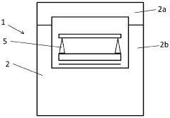
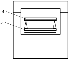
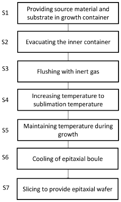
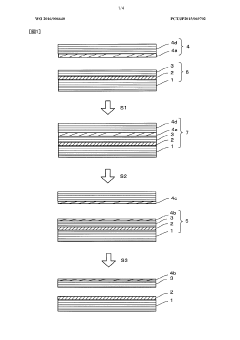
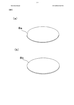
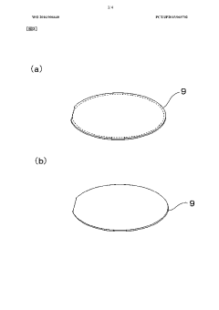
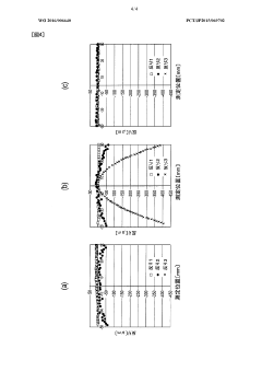
Production of silicon carbide epitaxial wafers
PatentWO2024117953A1
Innovation
- A method involving sublimation growth of a high-doping conductive layer on a low-doping monocrystalline SiC substrate, which avoids growing low-doped material on high-doped material, reducing stress and defect propagation, and allowing for improved doping homogeneity and crystalline quality, utilizing a physical vapor transport system with precise temperature control and dopant gas distribution.
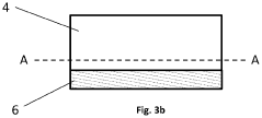
METHOD FOR PRODUCING SiC WAFER, METHOD FOR PRODUCING SiC SEMICONDUCTOR, AND SILICON CARBIDE COMPOSITE SUBSTRATE
PatentWO2016006640A1
Innovation
- A SiC wafer manufacturing method involving a silicon carbide composite substrate with a vitreous carbon layer and a CVD-SiC layer, where a single-crystal SiC substrate with an ion-implanted layer is bonded and then separated, allowing for the creation of thinner wafers with reduced ON resistance and enhanced mechanical strength.
Regulatory Compliance Requirements for SiC Manufacturing
Silicon Carbide (SiC) wafer manufacturing is subject to stringent regulatory frameworks that vary significantly across global markets. In the United States, the Environmental Protection Agency (EPA) enforces regulations under the Clean Air Act and Clean Water Act, specifically targeting the hazardous emissions and waste products generated during SiC production processes. Manufacturers must comply with National Emission Standards for Hazardous Air Pollutants (NESHAP) and obtain appropriate permits through the National Pollutant Discharge Elimination System (NPDES).
The European Union imposes even more rigorous standards through the Registration, Evaluation, Authorization and Restriction of Chemicals (REACH) regulation and the Restriction of Hazardous Substances (RoHS) Directive. SiC manufacturers operating in the EU must document the chemical substances used throughout the production process and demonstrate compliance with substance restrictions. Additionally, the Industrial Emissions Directive (IED) requires implementation of Best Available Techniques (BAT) to minimize environmental impact.
In Asia, Japan's Chemical Substances Control Law (CSCL) and China's Measures for Environmental Management of New Chemical Substances establish country-specific compliance requirements. These regulations often necessitate extensive documentation, testing, and certification processes before market entry is permitted.
Occupational safety regulations represent another critical compliance domain. The Occupational Safety and Health Administration (OSHA) in the US mandates specific workplace safety protocols for handling silicon carbide particulates and associated chemicals. Similar frameworks exist internationally, such as EU-OSHA guidelines and Japan's Industrial Safety and Health Law.
Quality certification standards, while not strictly regulatory, have become de facto requirements for market access. ISO 9001 certification is considered essential for SiC wafer manufacturers, while industry-specific standards like IATF 16949 for automotive applications impose additional compliance burdens for manufacturers targeting these sectors.
Emerging regulations around critical materials and supply chain security are increasingly impacting SiC manufacturing. The US CHIPS Act and similar initiatives in Europe and Asia establish new compliance requirements related to supply chain transparency, domestic production capabilities, and security of material sourcing.
Regulatory compliance costs represent a significant portion of operational expenses for SiC manufacturers, with estimates suggesting 15-20% of production costs are attributable to regulatory compliance activities. These costs include environmental monitoring systems, waste treatment facilities, certification processes, and specialized personnel for regulatory affairs management.
Environmental Impact Assessment of SiC Wafer Production
Silicon carbide (SiC) wafer production processes involve significant environmental considerations that must be thoroughly assessed to ensure sustainable manufacturing practices. The production of SiC wafers requires high-temperature processes, extensive energy consumption, and various chemicals that can potentially impact the environment if not properly managed. Current environmental impact assessments indicate that SiC wafer manufacturing generates approximately 30-40% more greenhouse gas emissions compared to traditional silicon wafer production, primarily due to the higher processing temperatures required.
Water usage represents another critical environmental concern, with estimates suggesting that a typical SiC wafer fabrication facility consumes between 4-7 million gallons of ultra-pure water daily. The wastewater from these processes contains various contaminants including heavy metals, acids, and polishing compounds that require specialized treatment systems before discharge.
Air quality impacts from SiC production stem primarily from the chemical vapor deposition processes that release particulate matter and volatile organic compounds. Recent studies have documented that facilities implementing state-of-the-art filtration systems can reduce these emissions by up to 95%, though implementation rates vary significantly across different geographical regions and regulatory environments.
Solid waste generation presents additional challenges, with an estimated 30-40% of raw SiC material becoming waste during wafer production. This includes off-specification wafers, grinding sludge, and polishing residues that may contain hazardous components requiring specialized disposal protocols.
Energy consumption remains perhaps the most significant environmental factor, with SiC wafer production facilities typically requiring 1.5-2 times the energy of comparable silicon wafer operations. The industry has begun implementing energy recovery systems that can recapture up to 25% of process heat, though these technologies remain in early adoption phases.
Life cycle assessments comparing SiC to traditional silicon technologies demonstrate that despite higher environmental impacts during production, SiC-based devices offer substantial environmental benefits during their operational lifetime. These benefits include energy savings of 15-30% in power electronics applications and extended device lifespans that reduce overall electronic waste generation.
Recent innovations in closed-loop water recycling systems have demonstrated potential to reduce freshwater consumption by up to 60% in SiC manufacturing facilities. Similarly, advances in process optimization have shown promising results in reducing material waste by 15-20% compared to earlier production methods, indicating positive trends toward more environmentally sustainable manufacturing practices.
Unlock deeper insights with Patsnap Eureka Quick Research — get a full tech report to explore trends and direct your research. Try now!
Generate Your Research Report Instantly with AI Agent
Supercharge your innovation with Patsnap Eureka AI Agent Platform!