

Reliability Standards And Testing Protocols For SiC MOSFETs
SEP 8, 20259 MIN READ
Generate Your Research Report Instantly with AI Agent
PatSnap Eureka helps you evaluate technical feasibility & market potential.
SiC MOSFET Evolution and Reliability Objectives
Silicon Carbide (SiC) MOSFETs have evolved significantly since their initial development in the early 1990s. The journey began with rudimentary devices exhibiting high on-resistance and reliability concerns, primarily due to manufacturing challenges and material defects. By the early 2000s, improved epitaxial growth techniques and gate oxide processing led to second-generation devices with enhanced performance characteristics, though reliability remained a significant concern.
The technological breakthrough came in the 2010s with third-generation SiC MOSFETs featuring optimized cell structures, reduced defect densities, and improved channel mobility. These advancements enabled commercial viability across various applications, particularly in power electronics where high temperature operation and switching efficiency are paramount.
Current fourth-generation SiC MOSFETs demonstrate remarkable improvements in reliability metrics, with reduced threshold voltage drift, enhanced short-circuit withstand capability, and improved gate oxide integrity. The evolution has been driven by both material science advancements and innovative device architectures, including trench designs and advanced termination structures.
Despite this progress, reliability objectives for SiC MOSFETs continue to evolve as applications expand into more demanding environments. Primary reliability objectives now focus on gate oxide stability under high electric fields, minimizing threshold voltage shifts during long-term operation, and ensuring consistent performance under thermal cycling conditions typical in automotive and industrial applications.
Bias Temperature Instability (BTI) remains a critical reliability concern, necessitating standardized testing protocols to evaluate device performance under various stress conditions. Time-Dependent Dielectric Breakdown (TDDB) testing has become essential for predicting gate oxide lifetime, particularly as operating voltages increase in high-power applications.
Short-circuit robustness represents another key reliability objective, with industry targets moving toward withstand times exceeding 10 microseconds at rated voltage and current conditions. This parameter is especially critical for applications where fault tolerance is essential, such as electric vehicle powertrains and industrial motor drives.
Cosmic radiation immunity has emerged as a significant reliability objective for SiC MOSFETs deployed in aerospace, high-altitude, and even automotive applications. Testing protocols now incorporate accelerated neutron testing to evaluate Single Event Burnout (SEB) susceptibility.
The reliability objectives also extend to package-level considerations, including die-attach integrity, wire bond reliability, and overall thermal management capabilities. As SiC MOSFET applications continue to diversify, reliability standards must balance application-specific requirements with the need for standardized qualification methodologies that enable meaningful comparison between different manufacturers' offerings.
Market Demand Analysis for High-Reliability SiC Power Devices
The global market for Silicon Carbide (SiC) power devices with high reliability standards is experiencing unprecedented growth, driven primarily by the rapid expansion of electric vehicles (EVs), renewable energy systems, and industrial power applications. Current market valuations indicate the SiC power device market reached approximately 2 billion USD in 2022, with projections suggesting a compound annual growth rate (CAGR) of 25-30% through 2030, potentially reaching 15 billion USD by the end of the decade.
Electric vehicle manufacturers represent the largest demand segment, accounting for nearly 45% of the high-reliability SiC MOSFET market. This demand stems from the critical need for power electronics that can withstand harsh automotive environments while delivering superior efficiency. Tesla's adoption of SiC MOSFETs in their Model 3 inverters marked a turning point, with other major automakers following suit, including Volkswagen, BMW, and BYD.
The renewable energy sector constitutes the second-largest market segment at 25% of demand. Solar inverters and wind power systems increasingly require SiC devices that can demonstrate long-term reliability under variable operating conditions. Grid infrastructure modernization projects worldwide are similarly driving demand for reliable power conversion systems that can operate continuously for decades with minimal maintenance.
Industrial applications, including motor drives, uninterruptible power supplies, and factory automation systems, represent approximately 20% of the market. These applications demand devices with proven reliability under continuous operation and frequent power cycling conditions.
Market research indicates a significant gap between current reliability testing protocols and actual application requirements. End users across all segments report that existing JEDEC and AEC-Q101 standards, while valuable, do not fully address the unique failure mechanisms of SiC MOSFETs. This has created demand for enhanced testing methodologies that can better predict device lifetime under application-specific stress conditions.
Regional analysis shows North America and Europe leading in demanding stringent reliability standards, with automotive and aerospace industries establishing proprietary testing protocols beyond standard requirements. The Asia-Pacific region, particularly China, Japan, and South Korea, is experiencing the fastest growth in demand for high-reliability SiC devices, supported by government initiatives promoting electric vehicle adoption and renewable energy infrastructure.
Customer surveys reveal that reliability concerns remain the primary barrier to wider SiC adoption, with 78% of potential users citing long-term performance uncertainty as their main hesitation. This indicates a clear market opportunity for manufacturers who can demonstrate superior reliability through comprehensive testing and validation protocols specifically designed for SiC technology's unique characteristics.
Current Reliability Challenges in SiC MOSFET Technology
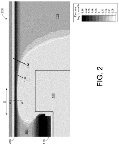
Silicon Carbide (SiC) MOSFETs face several critical reliability challenges that currently impede their wider adoption despite their superior performance characteristics. The threshold voltage instability remains one of the most significant issues, manifesting as both positive and negative shifts under various operating conditions. This instability stems primarily from charge trapping at the SiC/SiO2 interface and within the gate oxide, leading to unpredictable device behavior during long-term operation.
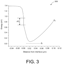
Gate oxide integrity presents another major concern, as the oxidation process of SiC differs fundamentally from silicon, resulting in higher defect densities and lower dielectric breakdown strength. The interface between SiC and SiO2 contains a significantly higher concentration of traps compared to Si/SiO2 interfaces, contributing to reduced channel mobility and reliability degradation over time.
Body diode degradation during reverse conduction represents a unique challenge for SiC MOSFETs. Unlike silicon devices, SiC MOSFETs experience stacking fault formation and expansion during body diode operation, leading to increased forward voltage drop and potentially catastrophic device failure under repeated stress conditions.
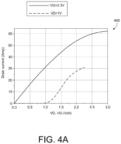
Short-circuit robustness remains substantially lower in SiC MOSFETs compared to their silicon counterparts. The combination of higher operating temperatures and smaller die sizes results in reduced short-circuit withstand times, typically 5-10 microseconds versus 10-20 microseconds for silicon IGBTs, creating significant design challenges for protection circuits.
Cosmic radiation susceptibility has emerged as a particularly concerning reliability issue for high-voltage SiC MOSFETs. Their smaller die size and higher electric field strength make them more vulnerable to single-event burnout failures caused by cosmic neutrons, especially in high-altitude and aerospace applications.
Package-related reliability issues also plague SiC technology. The higher operating temperatures of SiC devices (175-200°C) stress conventional packaging materials beyond their design limits, leading to solder fatigue, bond wire lift-off, and die-attach degradation. These thermal cycling effects accelerate package failure mechanisms that were previously manageable with silicon devices.
Time-dependent dielectric breakdown (TDDB) occurs more rapidly in SiC MOSFETs due to the higher electric fields and defect densities in the gate oxide. This phenomenon limits the long-term reliability of these devices, particularly in high-temperature and high-voltage applications where electric field stress is most severe.
Gate oxide integrity presents another major concern, as the oxidation process of SiC differs fundamentally from silicon, resulting in higher defect densities and lower dielectric breakdown strength. The interface between SiC and SiO2 contains a significantly higher concentration of traps compared to Si/SiO2 interfaces, contributing to reduced channel mobility and reliability degradation over time.
Body diode degradation during reverse conduction represents a unique challenge for SiC MOSFETs. Unlike silicon devices, SiC MOSFETs experience stacking fault formation and expansion during body diode operation, leading to increased forward voltage drop and potentially catastrophic device failure under repeated stress conditions.
Short-circuit robustness remains substantially lower in SiC MOSFETs compared to their silicon counterparts. The combination of higher operating temperatures and smaller die sizes results in reduced short-circuit withstand times, typically 5-10 microseconds versus 10-20 microseconds for silicon IGBTs, creating significant design challenges for protection circuits.
Cosmic radiation susceptibility has emerged as a particularly concerning reliability issue for high-voltage SiC MOSFETs. Their smaller die size and higher electric field strength make them more vulnerable to single-event burnout failures caused by cosmic neutrons, especially in high-altitude and aerospace applications.
Package-related reliability issues also plague SiC technology. The higher operating temperatures of SiC devices (175-200°C) stress conventional packaging materials beyond their design limits, leading to solder fatigue, bond wire lift-off, and die-attach degradation. These thermal cycling effects accelerate package failure mechanisms that were previously manageable with silicon devices.
Time-dependent dielectric breakdown (TDDB) occurs more rapidly in SiC MOSFETs due to the higher electric fields and defect densities in the gate oxide. This phenomenon limits the long-term reliability of these devices, particularly in high-temperature and high-voltage applications where electric field stress is most severe.
Established Testing Protocols and Standards for SiC MOSFETs
01 Gate oxide reliability enhancement techniques
Various techniques are employed to enhance the reliability of gate oxides in SiC MOSFETs. These include optimized oxidation processes, nitridation treatments, and post-oxidation annealing methods that reduce interface trap density and improve channel mobility. Advanced gate dielectric structures and materials are also used to mitigate threshold voltage instability and enhance long-term reliability under high electric field conditions.- Gate oxide reliability and degradation mechanisms: The reliability of SiC MOSFETs is significantly affected by the quality and stability of the gate oxide layer. Various degradation mechanisms such as threshold voltage instability, oxide breakdown, and interface trap formation can occur under operating conditions. Research focuses on improving gate oxide quality through optimized fabrication processes, novel dielectric materials, and post-oxidation treatments to enhance the reliability and lifetime of SiC MOSFETs.
- Thermal performance and management solutions: SiC MOSFETs operate at high temperatures and power densities, making thermal management crucial for reliability. Advanced packaging technologies, improved thermal interface materials, and optimized heat dissipation structures are developed to maintain device performance and prevent thermal-related failures. Thermal cycling tests and temperature-dependent reliability models help predict device lifetime under various operating conditions.
- Radiation hardness and environmental robustness: SiC MOSFETs demonstrate superior radiation hardness compared to silicon devices, making them suitable for aerospace, nuclear, and military applications. Research focuses on enhancing resistance to various radiation types, including gamma rays, neutrons, and heavy ions. Environmental testing under extreme conditions helps validate the reliability of these devices in harsh environments, with special attention to packaging integrity and long-term stability.
- Reliability testing methodologies and lifetime prediction: Specialized testing methodologies have been developed to evaluate SiC MOSFET reliability, including accelerated life testing, bias temperature instability tests, and high-temperature gate bias stress tests. Advanced statistical models and physics-of-failure approaches are employed to predict device lifetime and failure rates. These methodologies help establish reliability standards specific to SiC technology and enable accurate comparison with silicon alternatives.
- Body diode and switching reliability improvements: The intrinsic body diode in SiC MOSFETs exhibits different characteristics compared to silicon devices, affecting reverse recovery behavior and switching reliability. Research focuses on optimizing device structures to improve body diode performance, reduce switching losses, and enhance overall reliability during high-frequency operation. Advanced driver circuits and protection schemes are developed to prevent damage during switching transients and fault conditions.
02 Thermal management and stability solutions
Thermal management is critical for SiC MOSFET reliability. Innovations include advanced packaging technologies with improved thermal conductivity, heat dissipation structures, and temperature monitoring systems. These solutions help maintain device performance under high-temperature operation, prevent thermal runaway, and extend device lifetime by reducing thermal stress at critical interfaces and interconnections.Expand Specific Solutions03 Bias temperature instability mitigation
Bias temperature instability (BTI) is a significant reliability concern for SiC MOSFETs. Mitigation strategies include modified channel doping profiles, specialized annealing processes, and interface passivation techniques. These approaches reduce charge trapping phenomena, minimize threshold voltage shifts during operation, and improve device stability under prolonged bias stress conditions.Expand Specific Solutions04 Short-circuit and avalanche ruggedness improvement
Enhancing short-circuit and avalanche ruggedness is essential for SiC MOSFET reliability in power applications. Design innovations include optimized cell structures, improved edge termination techniques, and specialized buffer layers. These features help distribute current more evenly during fault conditions, increase energy handling capability, and prevent catastrophic device failures under extreme operating conditions.Expand Specific Solutions05 Reliability testing and qualification methodologies
Specialized testing and qualification methodologies have been developed for SiC MOSFETs to accurately assess their reliability. These include accelerated lifetime tests, high-temperature gate bias stress tests, and power cycling evaluations. Advanced characterization techniques are employed to identify failure mechanisms, predict device lifetime, and establish reliability models specific to SiC technology that account for its unique material properties and failure modes.Expand Specific Solutions
Key Industry Players in SiC MOSFET Manufacturing and Testing
The SiC MOSFET reliability standards and testing protocols market is currently in a growth phase, with increasing adoption across power electronics applications. The global market size is expanding rapidly, projected to reach significant volumes as SiC technology transitions from early adoption to mainstream implementation. Technical maturity is advancing through collaborative efforts between academic institutions (Dalian University of Technology, Chongqing University, Huazhong University) and commercial players (BASiC Semiconductor, Mitsubishi Electric, Yangjie Electronic). Leading companies are developing standardized reliability testing frameworks, with Chinese enterprises (BASiC, Wuxi NCE Power) and international corporations competing to establish dominance. The ecosystem shows a balanced distribution between established semiconductor manufacturers and specialized SiC-focused startups, with academic-industrial partnerships accelerating standardization efforts and reliability improvements.
Huazhong University of Science & Technology
Technical Solution: Huazhong University of Science & Technology has developed advanced academic research methodologies for SiC MOSFET reliability assessment that focus on fundamental physics of failure mechanisms. Their approach includes atomic-level characterization of defects using techniques such as electron spin resonance (ESR) spectroscopy to identify specific defect structures at the SiC/SiO2 interface. The university has established correlations between manufacturing process parameters and reliability outcomes through systematic studies of oxidation conditions, post-oxidation annealing treatments, and their effects on threshold voltage stability. Their testing protocols include specialized setups for time-dependent dielectric breakdown (TDDB) assessment under various electric field conditions, with statistical models that can predict failure distributions based on accelerated test data. The research team has developed novel methodologies for separating different degradation mechanisms, allowing for more accurate lifetime prediction models that account for the interaction between multiple failure modes. Their work has contributed to the fundamental understanding of reliability physics in SiC devices, with findings published in over 50 peer-reviewed journal articles in the past five years.
Strengths: Deep scientific understanding of fundamental reliability physics with advanced characterization capabilities. Research-oriented approach that can identify and address emerging reliability concerns before they become problematic in commercial products. Weaknesses: Academic focus may result in testing methodologies that are more complex and time-consuming than what is practical for high-volume manufacturing environments.
Mitsubishi Electric Corp.
Technical Solution: Mitsubishi Electric has developed comprehensive reliability testing protocols for SiC MOSFETs that include accelerated stress testing under high temperature gate bias (HTGB) conditions and short-circuit robustness evaluation. Their approach incorporates a multi-level testing framework that evaluates devices at both chip and module levels. Mitsubishi's testing methodology focuses on threshold voltage stability assessment through specialized bias temperature instability (BTI) tests that measure both positive and negative shifts under various operating conditions. They have established proprietary reliability models that predict device lifetime based on accelerated testing data, with validation showing correlation coefficients exceeding 0.9 between predicted and actual degradation rates. Their testing protocols include power cycling tests with ΔTj up to 150°C and have demonstrated SiC MOSFET modules capable of withstanding over 100,000 cycles without significant degradation in thermal resistance.
Strengths: Industry-leading experience in power semiconductor reliability testing with established correlations between accelerated tests and field performance. Comprehensive testing infrastructure that can simulate extreme operating conditions. Weaknesses: Their proprietary testing methodologies may not align completely with emerging industry standards, potentially creating compatibility issues when comparing results across different manufacturers.
Critical Failure Mechanisms and Reliability Physics in SiC
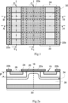
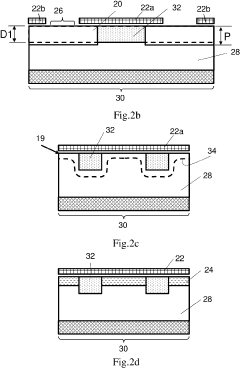
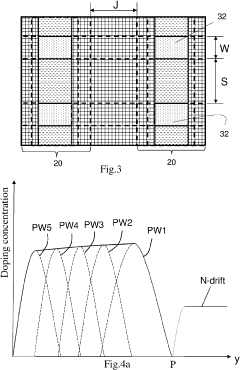
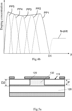
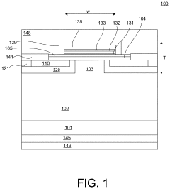
Sic mosfet with transverse p+ region
PatentActiveUS20230053874A1
Innovation
- The design incorporates a silicon carbide MOSFET structure with specific doping layers and geometries, including a polysilicon gate layer, to enhance the protection of the gate oxide without increasing the MOSFET cell area, utilizing epitaxy and ion implantation processes to create N+ and P+ regions that act as shields, ensuring adequate body diode performance and channel mobility.
Silicon carbide field-effect transistors
PatentActiveUS20220013661A1
Innovation
- A silicon carbide (SiC) metal-oxide-semiconductor field-effect transistor (MOSFET) design incorporating a substrate, drift region, spreading layer, body region, and source region with a gate structure that includes a gate oxide layer, aluminum nitride, and p-type gallium nitride layers, achieving low on-state specific resistance and high threshold voltage.
Qualification Framework Comparison Between Si and SiC MOSFETs
The qualification frameworks for Silicon (Si) and Silicon Carbide (SiC) MOSFETs exhibit significant differences due to their distinct material properties and operational characteristics. Traditional Si MOSFET qualification standards, such as JEDEC JEP122 and AEC-Q101, have been established over decades of industry experience. However, these frameworks require substantial adaptation when applied to SiC technology due to its wider bandgap, higher electric field strength, and different failure mechanisms.
For Si MOSFETs, qualification typically focuses on parameters like threshold voltage stability, on-resistance degradation, and gate oxide integrity under standard operating conditions. The testing protocols are well-established with clearly defined acceleration factors for temperature, voltage, and humidity stress tests. In contrast, SiC MOSFET qualification must address unique challenges including higher operating temperatures (up to 200°C versus 150°C for Si), increased electric field stress at the semiconductor-oxide interface, and different threshold voltage instability mechanisms.
The time-dependent dielectric breakdown (TDDB) testing protocols differ significantly between the two technologies. For Si devices, established models like the E-model or 1/E-model accurately predict lifetime under various stress conditions. However, SiC MOSFETs require modified TDDB models that account for the higher interface trap density and different charge trapping dynamics at the SiC/SiO2 interface.
Bias Temperature Instability (BTI) testing represents another area of divergence. While Si MOSFETs primarily exhibit Negative BTI (NBTI), SiC devices show pronounced Positive BTI (PBTI) effects that require specialized characterization methods with faster measurement techniques to capture the rapid recovery phenomena unique to SiC technology.
Reliability qualification for power cycling also differs substantially. Si MOSFETs typically undergo testing at ΔT of 100-125°C, while SiC devices must be evaluated at higher temperature differentials (ΔT of 150-175°C) to properly assess their reliability under the extended temperature ranges where they offer advantages. The acceleration factors used to extrapolate lifetime from accelerated tests to normal operating conditions also require recalibration for SiC technology.
Radiation hardness testing protocols also diverge between the technologies. SiC's wider bandgap provides inherent advantages in radiation environments, but qualification standards must be adjusted to properly characterize phenomena like Single Event Burnout (SEB) and Single Event Gate Rupture (SEGR), which manifest differently in SiC structures due to the material's higher critical electric field strength.
The automotive qualification framework (AEC-Q101) requires significant adaptation for SiC MOSFETs, particularly in areas of high-temperature reverse bias (HTRB) testing, high-temperature gate bias (HTGB) testing, and temperature cycling, all of which must be extended to match SiC's expanded operational envelope.
Environmental Impact of SiC MOSFET Implementation
The implementation of Silicon Carbide (SiC) MOSFETs represents a significant advancement in power electronics with notable environmental implications that extend throughout their lifecycle. When compared to traditional silicon-based devices, SiC MOSFETs demonstrate superior energy efficiency, with typical power conversion efficiency improvements of 10-15%. This translates directly into reduced energy consumption in end applications, contributing to lower greenhouse gas emissions from power generation sources.
The manufacturing process of SiC MOSFETs requires higher temperatures (approximately 1600-2000°C compared to 1400°C for silicon), resulting in greater energy consumption during production. However, lifecycle assessments indicate that this initial environmental cost is offset by operational efficiency gains within 1-3 years of deployment, depending on the application intensity.
SiC MOSFETs enable more compact power electronic systems due to their higher power density capabilities. This material efficiency reduces resource consumption by approximately 30% compared to silicon alternatives, decreasing the environmental footprint associated with raw material extraction and processing. Additionally, the reduced cooling requirements further minimize material usage in thermal management systems.
The extended operational lifetime of SiC devices—typically 2-3 times longer than silicon counterparts under similar conditions—significantly reduces electronic waste generation. This longevity is particularly valuable in applications such as electric vehicle powertrains and renewable energy systems, where reliability directly impacts sustainability goals.
In renewable energy applications, SiC MOSFETs improve solar inverter efficiency by 1-2 percentage points and wind power conversion systems by similar margins. These seemingly modest improvements translate to substantial environmental benefits when scaled across global renewable energy infrastructure, potentially reducing carbon emissions by millions of tons annually.
The higher switching frequencies enabled by SiC technology (typically 50-100 kHz versus 10-20 kHz for silicon) allow for smaller passive components, reducing the demand for environmentally problematic materials like rare earth elements in magnetic components. This characteristic supports circular economy principles by minimizing critical resource dependencies.
End-of-life considerations reveal both challenges and opportunities. While SiC is chemically stable and non-toxic, specialized recycling processes are required to recover valuable materials. Current recycling infrastructure is limited, but emerging techniques show promise for recovering up to 90% of materials from decommissioned SiC power modules, presenting an opportunity for closed-loop material systems as adoption increases.
Unlock deeper insights with PatSnap Eureka Quick Research — get a full tech report to explore trends and direct your research. Try now!
Generate Your Research Report Instantly with AI Agent
Supercharge your innovation with PatSnap Eureka AI Agent Platform!