Research on OLED vs MicroLED for Flexible Displays
OCT 24, 20259 MIN READ
Generate Your Research Report Instantly with AI Agent
PatSnap Eureka helps you evaluate technical feasibility & market potential.
Flexible Display Technology Evolution and Objectives
The evolution of flexible display technology represents a significant paradigm shift in the consumer electronics industry, transitioning from rigid glass-based displays to malleable interfaces that can bend, fold, and conform to various surfaces. This technological journey began in the early 2000s with rudimentary flexible electronic paper displays, progressing through several critical developmental phases to reach today's sophisticated flexible OLED implementations in commercial products.
The initial breakthrough came with the development of plastic substrates capable of replacing traditional glass, enabling fundamental flexibility while maintaining electronic functionality. By 2010, research institutions and technology companies had demonstrated early prototypes of flexible displays, though these suffered from significant limitations in durability, resolution, and manufacturing scalability.
The period between 2013 and 2017 marked accelerated advancement as OLED (Organic Light Emitting Diode) technology emerged as the dominant approach for flexible displays. OLED's self-emissive properties eliminated the need for rigid backlighting systems required by LCD technology, fundamentally enabling thinner and more flexible form factors. Samsung and LG Display pioneered commercial applications with curved OLED displays, establishing manufacturing processes that would later enable fully flexible implementations.
More recently, MicroLED has emerged as a promising alternative technology for flexible displays. Unlike OLED, which uses organic compounds that can degrade over time, MicroLED utilizes inorganic gallium nitride-based LEDs, potentially offering superior brightness, energy efficiency, and longevity. However, MicroLED faces significant manufacturing challenges, particularly in achieving the necessary pixel density on flexible substrates.
The primary objectives driving flexible display technology development include achieving greater durability through increased bend radius capabilities and bend cycle endurance. Current commercial flexible displays typically support between 100,000 to 200,000 fold cycles before showing degradation, while research targets aim to extend this to millions of cycles. Additionally, reducing the minimum bend radius from current commercial standards of 1-3mm to sub-millimeter levels remains a critical goal.
Other key objectives include improving optical performance metrics such as color gamut, contrast ratio, and brightness under deformation conditions; enhancing energy efficiency to address battery limitations in mobile devices; and developing cost-effective manufacturing processes to enable mass-market adoption beyond premium devices.
The convergence of these technological advancements aims to enable novel form factors and use cases, including rollable displays, stretchable interfaces, and conformable screens that can be integrated into non-traditional surfaces such as automotive interiors, wearable devices, and smart textiles.
Market Analysis for Flexible Display Applications
The flexible display market has witnessed remarkable growth in recent years, driven by increasing consumer demand for portable, lightweight, and durable electronic devices. As of 2023, the global flexible display market is valued at approximately 15.5 billion USD, with projections indicating a compound annual growth rate (CAGR) of 33.4% through 2028. This exponential growth trajectory underscores the significant market potential for both OLED and MicroLED technologies in flexible display applications.
Smartphones currently dominate the flexible display market, accounting for nearly 60% of total market share. Major manufacturers like Samsung, Apple, and Huawei have integrated flexible displays into their flagship devices, offering consumers innovative form factors such as foldable and rollable screens. The wearable technology segment follows as the second-largest application area, with smartwatches and fitness trackers increasingly adopting flexible display solutions to enhance user experience and device functionality.
Beyond consumer electronics, flexible displays are gaining traction in automotive dashboards, healthcare monitoring devices, and retail digital signage. The automotive sector, in particular, represents a high-growth opportunity, with premium vehicle manufacturers incorporating curved and conformable displays into their interior designs to enhance aesthetics and user interface capabilities.
Regional analysis reveals that Asia-Pacific leads the flexible display market, with South Korea, Japan, and China serving as manufacturing hubs and innovation centers. North America and Europe follow, primarily driven by high consumer adoption rates of premium electronic devices featuring flexible displays.
Consumer preference studies indicate that display quality, durability, and energy efficiency rank as the top three purchasing considerations for devices with flexible displays. OLED technology currently dominates the flexible display landscape due to its mature manufacturing processes and established supply chains. However, MicroLED is rapidly gaining attention for its superior brightness, longer lifespan, and potential for extreme flexibility in future applications.
Market barriers include high manufacturing costs, technical challenges in mass production, and concerns regarding long-term durability. The average price premium for devices with flexible displays remains approximately 30-40% higher than their rigid counterparts, though this gap is expected to narrow as manufacturing processes improve and economies of scale are achieved.
Industry analysts predict that as flexible display technologies mature, particularly with advances in MicroLED, new application markets will emerge, including transparent displays for augmented reality, ultra-thin displays for smart clothing, and large-format flexible displays for architectural applications. These emerging segments could potentially reshape the market landscape within the next five years.
OLED vs MicroLED: Current Status and Technical Barriers
OLED technology currently dominates the flexible display market due to its mature manufacturing processes and established supply chains. Major manufacturers like Samsung, LG Display, and BOE have invested heavily in OLED production facilities, achieving mass production capabilities with reasonable yields. OLED displays offer excellent color reproduction, high contrast ratios, and fast response times, making them suitable for various applications from smartphones to wearable devices.
However, OLED technology faces several significant challenges. The organic materials used in OLEDs degrade over time, leading to burn-in issues and limited lifespan, particularly for blue subpixels. This differential aging creates color shifts and reduces display longevity. Additionally, OLED efficiency remains suboptimal, with current devices converting only about 20-25% of input energy into visible light, resulting in higher power consumption.
MicroLED technology, though less mature, presents a promising alternative for flexible displays. These inorganic LED arrays offer superior brightness (up to 30 times brighter than OLEDs), better energy efficiency, and significantly longer lifespans without degradation issues. MicroLEDs also demonstrate excellent color gamut coverage and faster response times, potentially outperforming OLEDs in most technical specifications.
The primary barrier to MicroLED adoption in flexible displays is manufacturing complexity. The mass transfer process—moving millions of tiny LED chips precisely onto substrates—remains challenging at production scales. Current yield rates for MicroLED manufacturing hover around 70-80%, substantially lower than OLED's 90%+ yields. This manufacturing challenge directly impacts production costs, making MicroLED displays prohibitively expensive for mass-market applications.
Flexibility presents another technical hurdle for MicroLED. While OLED's organic nature inherently accommodates bending, MicroLED's inorganic materials require specialized engineering solutions to achieve comparable flexibility without compromising performance or durability. Researchers are exploring novel substrate materials and interconnect designs to address this limitation.
Both technologies face challenges in achieving truly transparent displays. OLED transparency is limited by the need for encapsulation layers and transistor arrays, while MicroLED transparency is constrained by the opaque nature of conventional LED structures and interconnects. Recent developments in transparent conductive materials show promise for both technologies but remain in early research stages.
Heat management represents another significant barrier, particularly for high-brightness applications. MicroLEDs generate substantial heat at maximum brightness levels, requiring advanced thermal management solutions for flexible form factors where traditional heat sinks are impractical. OLED displays face similar thermal challenges, though to a lesser extent due to their lower peak brightness capabilities.
Technical Comparison of OLED and MicroLED Solutions
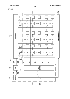
01 Flexible substrate technologies for OLED and MicroLED displays
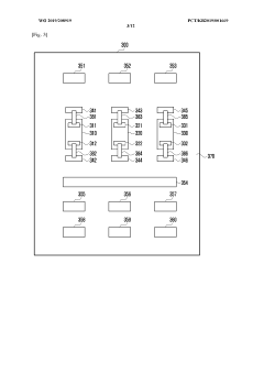
Flexible substrates are essential for creating bendable and foldable OLED and MicroLED displays. These substrates typically use materials like polyimide or ultra-thin glass that can withstand repeated bending while maintaining structural integrity. The manufacturing process involves depositing display components onto these flexible substrates using specialized techniques that preserve electrical connectivity during flexing. This technology enables displays that can be curved, folded, or rolled while maintaining optimal performance.- Flexible substrate technologies for OLED and MicroLED displays: Flexible substrates are essential for creating bendable and foldable OLED and MicroLED displays. These substrates typically use materials like polyimide or ultra-thin glass that can withstand repeated bending while maintaining structural integrity. The manufacturing process involves depositing display components on these flexible materials using specialized techniques that ensure electrical connectivity even during flexing. These technologies enable displays that can be curved, folded, or rolled while maintaining optimal performance.
- Transfer techniques for flexible MicroLED arrays: Advanced transfer techniques are crucial for placing MicroLED elements onto flexible substrates. These methods include mass transfer processes that can simultaneously position thousands of tiny LED chips with high precision. Specialized adhesives and bonding technologies ensure that the MicroLEDs remain securely attached even when the display is flexed or bent. These transfer techniques must accommodate the mechanical stress that occurs during bending while maintaining perfect pixel alignment and electrical connectivity.
- Encapsulation methods for flexible display protection: Flexible OLED and MicroLED displays require specialized encapsulation methods to protect sensitive electronic components from oxygen and moisture while maintaining flexibility. Thin-film encapsulation technologies create ultra-thin barrier layers that can bend without cracking. These methods often employ alternating organic and inorganic layers to provide effective protection while allowing the display to flex. Advanced encapsulation techniques are essential for ensuring the longevity and reliability of flexible display technologies in various environmental conditions.
- Interconnect solutions for flexible display circuits: Specialized interconnect technologies are developed to maintain electrical connectivity in flexible OLED and MicroLED displays during bending and folding. These include stretchable conductive materials, serpentine circuit patterns, and novel bonding techniques that can withstand repeated mechanical stress. The interconnect solutions must balance electrical performance with mechanical flexibility, ensuring stable pixel addressing and power delivery even when the display is deformed. These technologies are critical for creating truly flexible display systems that can operate reliably in various form factors.
- Backplane technologies for flexible displays: Flexible backplane technologies enable the active matrix driving of OLED and MicroLED displays on bendable substrates. These include thin-film transistor (TFT) arrays made with materials like low-temperature polysilicon (LTPS) or metal oxide semiconductors that can maintain performance while being flexed. Advanced backplane designs incorporate stress-relief structures that prevent circuit failure during bending. The backplane must provide stable pixel driving while accommodating the mechanical deformation that occurs in flexible display applications.
02 Encapsulation methods for flexible display protection
Advanced encapsulation techniques are crucial for protecting flexible OLED and MicroLED displays from environmental factors while maintaining flexibility. These methods include thin-film encapsulation using alternating organic and inorganic layers, which create an effective moisture and oxygen barrier while remaining bendable. Some approaches utilize specialized adhesives and composite materials that can flex without cracking. These protection systems are essential for ensuring the longevity and reliability of flexible display technologies in various applications.Expand Specific Solutions03 Interconnect technologies for flexible displays
Specialized interconnect technologies are developed to maintain electrical connectivity in flexible OLED and MicroLED displays during bending and folding. These include stretchable conductive materials, serpentine circuit patterns that can extend without breaking, and novel bonding techniques that accommodate movement. Some approaches use liquid metal or conductive polymers that maintain conductivity when deformed. These interconnect solutions are critical for ensuring consistent performance across the entire display surface even when flexed.Expand Specific Solutions04 Transfer processes for MicroLED on flexible substrates
Innovative transfer processes have been developed to place MicroLED elements onto flexible substrates without damage. These methods include mass transfer techniques using temporary carrier substrates, selective laser transfer systems, and electrostatic or adhesive-based approaches. The processes must precisely position thousands of tiny LED elements while accommodating the mechanical properties of flexible materials. These transfer technologies are key to manufacturing high-resolution, flexible MicroLED displays with uniform brightness and color consistency.Expand Specific Solutions05 Stress compensation and mechanical durability solutions
Various technologies address the mechanical stress challenges in flexible OLED and MicroLED displays. These include stress-neutral layer designs, specialized buffer layers that absorb deformation forces, and composite structures that distribute stress evenly. Some approaches incorporate self-healing materials or reinforcement patterns at high-stress points. Testing methodologies have been developed to evaluate and improve the durability of these displays under repeated bending, folding, or rolling conditions, ensuring long-term reliability in consumer products.Expand Specific Solutions
Key Industry Players in Flexible Display Manufacturing
The flexible display market is currently in a transitional growth phase, with OLED technology dominating but MicroLED emerging as a promising alternative. The global market is expanding rapidly, projected to reach $15-20 billion by 2025, driven by demand for foldable smartphones and wearable devices. While OLED technology has achieved commercial maturity with companies like Samsung Display, LG Display, and BOE Technology leading production, MicroLED remains in early commercialization stages. Samsung Electronics and BOE are investing heavily in MicroLED development, while Universal Display Corporation and Lumileds Singapore are advancing core technologies. Chinese manufacturers including TCL China Star and Tianma Microelectronics are rapidly closing the technology gap with established players, particularly in OLED manufacturing capabilities.
BOE Technology Group Co., Ltd.
Technical Solution: BOE has developed advanced flexible OLED technology utilizing LTPO (Low-Temperature Polycrystalline Oxide) backplanes that enable variable refresh rates from 1-120Hz, significantly reducing power consumption by up to 30% compared to conventional displays[1]. Their flexible OLED panels incorporate a multi-layer structure with ultra-thin glass substrates (as thin as 0.03mm) and specialized encapsulation technology to achieve bending radii below 1mm without performance degradation[2]. For MicroLED development, BOE employs mass transfer technology capable of placing millions of microscopic LED chips with precision below 1μm, achieving pixel densities exceeding 1000PPI for flexible applications. Their proprietary compensation algorithms address the uniformity challenges inherent in MicroLED, maintaining color accuracy across flexible surfaces even when bent[3]. BOE has also pioneered stretchable display technology that can extend up to 15% while maintaining electrical performance through specialized serpentine circuit designs and elastic substrate materials.
Strengths: Industry-leading production capacity for flexible OLED with established mass production capabilities; Strong IP portfolio in flexible display encapsulation technology; Advanced in-house backplane technology. Weaknesses: MicroLED technology still in early commercialization phase with higher production costs than competitors; Yield rates for flexible MicroLED remain challenging at scale.
Prilit Optronics, Inc.
Technical Solution: Prilit Optronics has developed specialized flexible display technology focusing on ultra-thin form factors through their proprietary "NanoMesh" electrode system, which replaces traditional ITO with a flexible metal nanowire network achieving transparency above 92% while maintaining conductivity below 20 ohms/square even when flexed[1]. Their flexible display architecture incorporates a unique "stress-neutral layer" design that positions active elements at the mechanical neutral plane, enabling bending radii below 1mm without performance degradation. For MicroLED flexible displays, Prilit employs a distinctive "self-aligned transfer" process that utilizes electrostatic forces to precisely position micro-scale LED chips onto flexible substrates with alignment accuracy below 0.5μm[2]. Their flexible MicroLED panels incorporate specialized phosphor-converted blue MicroLEDs that achieve wider color gamut (>90% Rec.2020) while simplifying the manufacturing process compared to discrete RGB approaches. Prilit has also developed proprietary encapsulation technology using alternating organic/inorganic layers that achieves water vapor transmission rates below 10^-6 g/m²/day while maintaining flexibility, addressing a critical reliability challenge for flexible displays[3].
Strengths: Specialized expertise in ultra-thin flexible display architectures; Innovative electrode and encapsulation technologies; Agile R&D approach enabling rapid prototyping. Weaknesses: Limited production capacity compared to larger manufacturers; Less vertical integration requiring partnerships for mass production; Narrower product portfolio focused primarily on specialized applications.
Patent Landscape and Breakthrough Innovations
Flexible display and method for manufacturing the same
PatentInactiveUS20140097417A1
Innovation
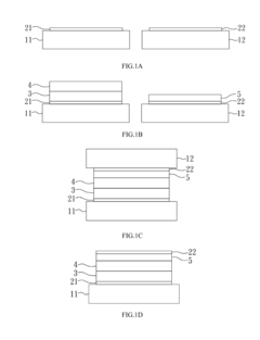
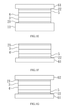
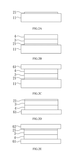
- A flexible display structure comprising a carrier, an interface layer with a thickness of 0.5 μm to 10 μm, and an organic light-emitting diode layer, where the interface layer is formed using materials like polyimide, silicon nitride, or gallium nitride, and the substrate is replaced with a carrier using conventional techniques, reducing the need for expensive substrates and coating equipment.

LED display and electronic device having same
PatentWO2019208919A1
Innovation
- The development of a micro-LED display with a bezel-less design and segmentation capabilities, allowing for flexible displays of various sizes, achieved through direct mounting of micro-LEDs on a substrate and innovative electrical connections using conductive patterns and wiring lines, enabling robust electrical connections and flexible display configurations.
Manufacturing Processes and Scalability Challenges
The manufacturing processes for OLED and MicroLED technologies present distinct challenges that significantly impact their commercial viability for flexible display applications. OLED manufacturing has matured considerably over the past decade, with established processes for both rigid and flexible implementations. The primary OLED production method involves vacuum thermal evaporation for small molecule OLEDs or solution processing for polymer-based variants. For flexible OLED displays, manufacturers have developed specialized thin-film encapsulation techniques to protect organic materials from oxygen and moisture while maintaining flexibility.
In contrast, MicroLED manufacturing remains in earlier development stages, facing more substantial scalability hurdles. The process requires precise transfer of millions of microscopic LED chips from semiconductor wafers to display substrates with near-perfect yield rates. Current pick-and-place methods struggle with throughput limitations when handling the massive number of sub-10μm LED elements required for high-resolution displays. Mass transfer techniques show promise but still face challenges in alignment accuracy and consistency across large areas.
Yield management represents a critical differentiator between these technologies. OLED manufacturing has achieved relatively high yields through process optimization, though still experiences challenges with pixel defects in large-format displays. MicroLED production currently suffers from significantly lower yields, with estimates suggesting that even small defect rates can render entire displays unusable due to the sheer number of individual LED elements involved.
Cost structures also differ substantially. OLED manufacturing benefits from economies of scale and established supply chains, though high-end flexible variants still command premium pricing. MicroLED production costs remain prohibitively high for mass-market applications, primarily due to complex transfer processes, stringent quality control requirements, and lower yields. Industry analysts estimate MicroLED manufacturing costs at 2-5 times that of comparable OLED displays at current technology readiness levels.
Equipment infrastructure presents another key consideration. OLED production leverages modified semiconductor manufacturing equipment, with major investments already made by display manufacturers. MicroLED requires development of specialized equipment for handling microscopic LED elements at unprecedented scales, representing significant capital expenditure before mass production becomes viable. Several equipment manufacturers are developing dedicated MicroLED production tools, but standardization remains limited.
For flexible applications specifically, both technologies face additional manufacturing complexities. OLED has demonstrated commercial viability in flexible form factors, though durability and folding radius limitations persist. MicroLED's potential advantages in flexibility remain largely theoretical, with significant engineering challenges in creating robust connections between rigid LED elements on flexible substrates while maintaining electrical and optical performance.
Energy Efficiency and Environmental Impact Assessment
Energy efficiency represents a critical factor in the evaluation of display technologies, particularly when comparing OLED and MicroLED for flexible display applications. OLED displays demonstrate significant energy advantages in dark-content scenarios due to their self-emissive nature, where black pixels consume virtually no power. This characteristic makes OLEDs particularly efficient for mobile applications with predominantly dark interfaces. However, when displaying bright or white content, OLEDs typically consume more power than alternative technologies.
MicroLED technology promises superior energy efficiency across a broader range of content types. Initial research indicates potential energy savings of 30-50% compared to OLEDs when displaying mixed content. This efficiency stems from MicroLED's higher luminous efficacy, with laboratory prototypes achieving up to 200 lumens per watt versus OLED's typical 100-150 lumens per watt range. The efficiency gap widens further when considering operational longevity, as MicroLED displays maintain their efficiency levels longer than OLEDs, which experience gradual degradation.
From an environmental impact perspective, manufacturing processes for both technologies present distinct challenges. OLED production involves organic compounds and solvents that require careful handling and disposal. The manufacturing yield rates for flexible OLEDs remain lower than rigid displays, resulting in increased material waste. Additionally, the shorter lifespan of OLED displays (typically 30,000-50,000 hours before significant brightness degradation) contributes to electronic waste concerns.
MicroLED manufacturing currently faces yield challenges at scale, particularly for high-resolution flexible applications. However, the technology utilizes fewer rare earth elements and toxic materials compared to some display alternatives. The extended operational lifespan of MicroLED displays—projected to exceed 100,000 hours—significantly reduces replacement frequency and associated electronic waste generation.
Carbon footprint analysis reveals that power consumption during the use phase constitutes approximately 70% of the lifecycle environmental impact for both technologies. MicroLED's potential energy efficiency advantage could therefore translate to meaningful environmental benefits over product lifetimes. Recent lifecycle assessments suggest that a 30% reduction in energy consumption could reduce carbon emissions by approximately 25-35 kg CO2 equivalent per device over a three-year usage period.
Water usage represents another important environmental consideration, with OLED manufacturing typically requiring 20-30% more water than comparable LCD processes. Early MicroLED production data suggests similar water requirements to LCD manufacturing, though optimization efforts continue as the technology matures toward mass production.
Unlock deeper insights with PatSnap Eureka Quick Research — get a full tech report to explore trends and direct your research. Try now!
Generate Your Research Report Instantly with AI Agent
Supercharge your innovation with PatSnap Eureka AI Agent Platform!