SiC MOSFET Degradation Mechanisms Under Repetitive Stress
SEP 8, 20259 MIN READ
Generate Your Research Report Instantly with AI Agent
Patsnap Eureka helps you evaluate technical feasibility & market potential.
SiC MOSFET Evolution and Research Objectives
Silicon Carbide (SiC) MOSFET technology has evolved significantly over the past three decades, transforming from a laboratory curiosity to a commercial reality that is revolutionizing power electronics. The journey began in the early 1990s with rudimentary SiC devices exhibiting poor channel mobility and high defect densities. By the early 2000s, researchers had made substantial progress in crystal growth techniques, reducing micropipe densities from over 100/cm² to below 1/cm², enabling the first commercially viable devices.
The technological evolution accelerated in the 2010s with the introduction of second-generation SiC MOSFETs featuring improved gate oxide reliability and reduced on-resistance. This period marked the transition from niche applications to broader market adoption, particularly in automotive and industrial sectors. Current fourth-generation devices boast significantly enhanced performance metrics, including lower switching losses, higher temperature operation capabilities up to 200°C, and blocking voltages exceeding 10kV.
Despite these advancements, SiC MOSFETs face reliability challenges under repetitive stress conditions that limit their full potential. The primary degradation mechanisms include threshold voltage instability, gate oxide deterioration, and body diode degradation during repetitive switching events. These issues become particularly pronounced in applications requiring high-frequency operation or those subject to frequent power cycling.
Understanding these degradation mechanisms is crucial as SiC MOSFETs continue to penetrate critical applications in electric vehicles, renewable energy systems, and industrial drives. The technology's promise of higher efficiency, reduced cooling requirements, and smaller system footprints can only be fully realized when long-term reliability concerns are adequately addressed.
The research objectives in this field are multifaceted. First, there is a need to develop comprehensive models that accurately predict device degradation under various stress conditions, enabling more reliable lifetime estimations. Second, researchers aim to identify the fundamental physical mechanisms responsible for parameter shifts during repetitive stress, particularly at the SiC/SiO2 interface where many reliability issues originate.
Additionally, research efforts are focused on developing improved fabrication techniques and novel device structures that enhance resilience against repetitive stress. This includes exploration of alternative gate dielectrics, channel doping profiles, and edge termination designs that minimize electric field concentrations at critical regions within the device structure.
The ultimate goal is to establish standardized reliability testing protocols specifically tailored for SiC technology, as current silicon-based testing methodologies may not adequately capture the unique degradation mechanisms in wide bandgap semiconductors. These efforts collectively aim to enable SiC MOSFETs to achieve their theoretical performance limits while maintaining reliability standards necessary for mission-critical applications.
Market Demand Analysis for SiC Power Devices
The Silicon Carbide (SiC) power device market is experiencing unprecedented growth, driven by the increasing demand for high-efficiency power electronics across multiple industries. The global SiC power semiconductor market, valued at approximately $1.4 billion in 2022, is projected to reach $6.3 billion by 2028, representing a compound annual growth rate (CAGR) of over 28%. This remarkable growth trajectory underscores the critical importance of addressing degradation mechanisms in SiC MOSFETs to ensure long-term reliability.
Electric vehicle (EV) applications constitute the largest market segment for SiC power devices, accounting for roughly 60% of the total market share. The automotive industry's shift toward electrification has created substantial demand for SiC MOSFETs due to their superior performance in high-temperature, high-frequency, and high-voltage applications. Major automotive manufacturers have announced plans to increase SiC content in their vehicles by 25-30% annually through 2026, highlighting the growing market pull.
Industrial power supplies represent the second-largest application segment, comprising approximately 18% of the market. The industrial sector values SiC MOSFETs for their ability to reduce energy losses by up to 50% compared to traditional silicon-based alternatives. This efficiency advantage translates directly to operational cost savings, driving adoption despite higher initial investment costs.
Renewable energy systems, particularly solar inverters and wind power converters, constitute about 15% of the SiC power device market. The push for greater energy efficiency and power density in these applications has accelerated SiC adoption, with the solar inverter segment growing at 32% annually—faster than the overall market average.
Market research indicates that concerns about long-term reliability under repetitive stress conditions remain a significant barrier to wider adoption. Approximately 42% of potential industrial users cite reliability uncertainties as their primary hesitation factor. This underscores the critical importance of understanding degradation mechanisms in SiC MOSFETs under repetitive stress conditions.
Regional analysis shows North America and Europe leading in SiC adoption for automotive applications, while Asia-Pacific dominates in industrial and consumer electronics implementations. China has emerged as both the largest consumer and producer of SiC power devices, with government initiatives supporting domestic manufacturing capacity expansion by 300% between 2021 and 2025.
The market demand for enhanced reliability in SiC MOSFETs is evidenced by premium pricing for devices with demonstrated robustness under repetitive stress conditions. Products with verified reliability command price premiums of 15-20% over standard offerings, indicating strong market willingness to pay for performance assurance in critical applications.
Current Challenges in SiC MOSFET Reliability
Despite significant advancements in Silicon Carbide (SiC) MOSFET technology, several critical reliability challenges persist that impede its widespread adoption in high-power and high-temperature applications. The primary concern remains the oxide interface quality, which is fundamentally different from traditional silicon devices. The SiC/SiO2 interface exhibits a higher density of interface traps, particularly near the conduction band edge, leading to reduced channel mobility and threshold voltage instability under repetitive stress conditions.
Threshold voltage (Vth) instability presents a significant challenge, manifesting as both positive and negative shifts depending on the stress conditions. Under positive bias temperature instability (PBTI), electrons become trapped in the gate oxide, causing positive Vth shifts. Conversely, negative bias temperature instability (NBTI) results in hole trapping and negative Vth shifts. These bidirectional shifts complicate device performance prediction in real-world applications where cycling between operating states occurs frequently.
Time-dependent dielectric breakdown (TDDB) represents another critical reliability concern. The higher electric fields required for SiC MOSFET operation, combined with the inherent defects at the SiC/SiO2 interface, accelerate oxide degradation. This phenomenon is particularly problematic in repetitive stress scenarios, where cumulative damage to the gate oxide can lead to premature device failure.
Body diode degradation under repetitive switching presents a unique challenge for SiC MOSFETs. Unlike silicon devices, SiC MOSFETs experience significant forward voltage drift in their intrinsic body diodes after repetitive reverse conduction events. This degradation is attributed to stacking fault expansion and basal plane dislocations that propagate through the epitaxial layer during reverse conduction.
Short-circuit robustness remains inferior compared to silicon IGBTs, with typical withstand times of only 5-10 microseconds versus 10-20 microseconds for silicon counterparts. This limitation stems from SiC's smaller die size and higher current density, resulting in faster temperature rises during fault conditions. The repetitive short-circuit capability is particularly concerning, as each event causes cumulative damage to the gate oxide and drift region.
Temperature-dependent parameter shifts pose significant modeling challenges. SiC MOSFETs exhibit more pronounced parameter variations with temperature than silicon devices, including non-linear changes in on-resistance, threshold voltage, and switching characteristics. These variations become more complex after repetitive stress, as degradation mechanisms accelerate at elevated temperatures.
Packaging-related failures have emerged as a significant reliability bottleneck. The rapid switching capability of SiC MOSFETs induces higher thermomechanical stress on die-attach materials and wire bonds. Under repetitive operation, especially in applications with frequent temperature cycling, these stresses can lead to solder fatigue, wire bond lift-off, and ultimately package failure.
Existing Degradation Mitigation Strategies
01 Threshold voltage instability and oxide degradation
SiC MOSFETs experience threshold voltage instability due to charge trapping at the SiC/SiO2 interface. This degradation mechanism is characterized by shifts in threshold voltage during operation, particularly under high temperature and bias stress conditions. The oxide layer deteriorates over time due to defect generation and charge accumulation, leading to reduced reliability and performance. This mechanism is particularly prominent in SiC devices due to the higher interface trap density compared to silicon-based MOSFETs.- Threshold voltage instability and oxide degradation: SiC MOSFETs experience threshold voltage instability due to charge trapping at the SiC/SiO2 interface. This degradation mechanism is characterized by shifts in threshold voltage during device operation, particularly under high temperature and bias stress conditions. The oxide layer degradation is accelerated by high electric fields and thermal stress, leading to increased leakage current and reduced reliability over time. Interface traps and fixed charges in the gate oxide contribute significantly to this degradation mechanism.
- Body diode degradation and forward voltage drift: The body diode in SiC MOSFETs undergoes degradation during operation, particularly during reverse recovery. This results in increased forward voltage drop and switching losses over time. The degradation is attributed to the formation of stacking faults and basal plane dislocations in the SiC crystal structure. These defects propagate under electrical and thermal stress conditions, leading to increased on-resistance and reduced current handling capability of the device.
- Short-circuit reliability and thermal degradation: SiC MOSFETs are susceptible to degradation under short-circuit conditions due to their reduced chip area and higher current density compared to silicon devices. The high temperature generated during short-circuit events can cause permanent damage to the gate oxide and drift region. Thermal cycling and power cycling lead to mechanical stress at material interfaces, resulting in package-related failures such as bond wire lift-off and solder fatigue. These thermal degradation mechanisms significantly impact the long-term reliability of SiC MOSFETs in power applications.
- Channel mobility reduction and interface trap generation: The channel mobility in SiC MOSFETs degrades over time due to the generation of interface traps at the SiC/SiO2 boundary. This degradation mechanism is accelerated by high-temperature operation and gate bias stress. The interface trap density increases with device operation, leading to reduced channel mobility, increased on-resistance, and degraded switching performance. Various defects at the semiconductor-oxide interface contribute to this degradation, including carbon clusters and silicon vacancies.
- Gate oxide reliability and time-dependent dielectric breakdown: The gate oxide in SiC MOSFETs is prone to time-dependent dielectric breakdown (TDDB) due to the high electric fields applied across the thin oxide layer. This degradation mechanism involves the formation of conductive paths through the oxide, eventually leading to catastrophic failure. The breakdown process is accelerated by defects in the oxide layer, high-temperature operation, and voltage stress. The quality of the SiC/SiO2 interface plays a crucial role in determining the long-term reliability of the gate oxide structure.
02 Channel mobility degradation
The mobility of carriers in the channel region of SiC MOSFETs degrades over time due to increased scattering mechanisms. This degradation is caused by interface roughness, coulomb scattering from charged interface traps, and phonon scattering at elevated temperatures. The reduction in channel mobility leads to increased on-resistance and decreased current capability of the device. This mechanism is particularly significant in SiC MOSFETs due to the inherently lower mobility of carriers in SiC compared to silicon.Expand Specific Solutions03 Body diode degradation and bipolar degradation
The body diode in SiC MOSFETs experiences degradation during reverse conduction, leading to increased forward voltage drop and switching losses. This degradation is attributed to the formation and expansion of stacking faults in the SiC crystal structure. Additionally, bipolar degradation occurs due to recombination-induced defects during minority carrier injection, causing an increase in on-resistance and reduction in device performance over time. These mechanisms are particularly problematic in applications requiring frequent reverse conduction or hard switching conditions.Expand Specific Solutions04 Gate oxide reliability under high electric field
SiC MOSFETs are susceptible to gate oxide breakdown under high electric field stress due to the higher critical field strength of SiC compared to silicon. The gate oxide reliability is compromised by time-dependent dielectric breakdown, stress-induced leakage current, and hot carrier injection. These phenomena lead to increased gate leakage current, reduced breakdown voltage, and eventually catastrophic device failure. The thinner gate oxides used in modern SiC MOSFETs to achieve lower on-resistance make this degradation mechanism more pronounced.Expand Specific Solutions05 Thermal cycling and packaging-related degradation
SiC MOSFETs undergo degradation due to thermal cycling and packaging-related issues. The coefficient of thermal expansion mismatch between SiC die, die attach material, and substrate leads to mechanical stress, which can cause die cracking, bond wire fatigue, and solder joint degradation. Additionally, high-temperature operation accelerates various failure mechanisms including metal migration, intermetallic compound formation, and package delamination. These degradation mechanisms affect the thermal performance and long-term reliability of SiC MOSFETs, particularly in applications with frequent temperature fluctuations.Expand Specific Solutions
Leading Manufacturers and Research Institutions
The SiC MOSFET degradation mechanisms market is currently in a growth phase, with increasing adoption of wide bandgap semiconductors in power electronics. The global market size for SiC power devices is expanding rapidly, projected to reach $2.5 billion by 2025 with a CAGR of 30%. The technology maturity varies across players, with established companies like Infineon Technologies, STMicroelectronics, and Mitsubishi Electric leading with mature reliability testing frameworks. Emerging competitors including BASiC Semiconductor, Tower Semiconductor, and PN Junction Semiconductor are advancing quickly, particularly in China's growing ecosystem. Academic institutions such as Dalian University of Technology and Fudan University are contributing significant research on degradation mechanisms, while industrial-academic collaborations between companies like Samsung Electronics and research institutes are accelerating understanding of long-term reliability challenges under repetitive stress conditions.
Mitsubishi Electric Corp.
Technical Solution: Mitsubishi Electric has developed a comprehensive approach to mitigating SiC MOSFET degradation under repetitive stress conditions. Their technology incorporates a specialized gate oxide formation process with precise control of oxidation parameters and post-oxidation treatments to minimize interface trap generation. Mitsubishi's SiC MOSFETs feature an optimized cell structure with reduced electric field concentrations at the gate oxide interface, significantly decreasing hot carrier injection effects during repetitive switching. The company has implemented advanced screening methodologies that identify devices susceptible to bias temperature instability (BTI) effects, ensuring more consistent long-term performance. Their devices include built-in protection features that monitor critical parameters like junction temperature and gate voltage transients in real-time, allowing for adaptive control strategies that extend device lifetime. Additionally, Mitsubishi has developed specialized gate driver solutions with precise control of switching transients to minimize stress during high-frequency operation.
Strengths: Excellent long-term reliability under repetitive switching conditions; comprehensive integration of protection features in both device and system-level solutions. Weaknesses: Higher initial cost compared to conventional silicon solutions; requires more complex thermal management systems for optimal reliability performance.
Stmicroelectronics Srl
Technical Solution: STMicroelectronics has developed a multi-layered approach to address SiC MOSFET degradation under repetitive stress. Their technology incorporates a proprietary gate oxide formation process that significantly reduces interface trap density, a primary factor in threshold voltage instability. ST's SiC MOSFETs feature an advanced trench design with optimized corner radius and dielectric thickness distribution to minimize electric field crowding during switching transients. The company has implemented a unique post-oxidation annealing technique that reduces oxide defects by approximately 40% compared to conventional processes. Their devices include built-in temperature and current sensors that enable real-time monitoring of degradation indicators. ST has also developed specialized gate driver solutions with precise control of dV/dt and dI/dt to minimize stress during repetitive switching operations, extending device lifetime by up to 30% in high-frequency applications.
Strengths: Excellent threshold voltage stability under repetitive stress; comprehensive integration of protection features in both device and driver solutions. Weaknesses: Performance optimization focuses primarily on automotive applications, potentially limiting suitability for some industrial power conversion scenarios; higher cost structure compared to silicon alternatives.
Key Failure Mechanisms Under Repetitive Stress
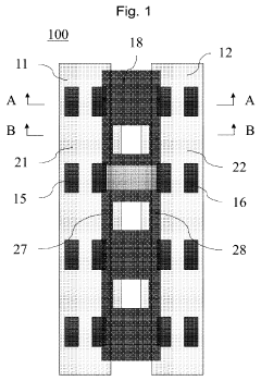
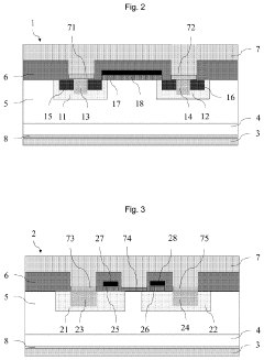
Silicon carbide metal oxide semiconductor field effect transistor and manufacturing method of silicon carbide metal oxide semiconductor field effect transistor
PatentPendingUS20230378341A1
Innovation
- The design incorporates alternating cells with specific well regions, source regions, and contact layers, including ohmic and Schottky contacts, to reduce channel density, enhance short-circuit tolerance, and minimize reverse leakage current and forward voltage drop, while maintaining the transistor's size and functionality.
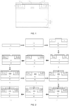
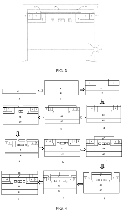
Silicon carbide metal oxide semiconductor field effect transistor and manufacturing method therefor
PatentInactiveEP3813127A1
Innovation
- A silicon carbide metal-oxide-semiconductor field-effect transistor structure is developed, incorporating a second conduction type epitaxial layer, first conduction type well regions, and additional doping regions within the JFET region to reduce gate oxide electric field strength, including a gate oxide layer and passivation protection, with specific doping concentrations and geometries to enhance device performance.
Reliability Testing Standards and Methodologies
The reliability testing of SiC MOSFETs requires standardized methodologies to ensure consistent evaluation across different devices and manufacturers. Currently, several established standards govern the reliability assessment of power semiconductor devices, with specific adaptations for SiC technology due to its unique material properties and degradation mechanisms.
The Joint Electron Device Engineering Council (JEDEC) has developed key standards including JESD22-A108 for temperature cycling, JESD22-A110 for highly accelerated temperature and humidity stress test (HAST), and JESD47 for stress-test-driven qualification of integrated circuits. These standards provide foundational frameworks that have been modified to address SiC MOSFET-specific concerns.
International Electrotechnical Commission (IEC) standards also play a crucial role, particularly IEC 60747-8 for semiconductor devices and IEC 60749 for semiconductor device mechanical and climatic test methods. These standards outline procedures for evaluating device robustness under various environmental and electrical stresses.
For repetitive stress testing specifically, methodologies focus on three primary categories: thermal cycling, power cycling, and gate stress testing. Thermal cycling tests (typically -55°C to +150°C or higher for SiC) evaluate package integrity and die attachment reliability. Power cycling tests assess device performance under repetitive on-off switching conditions with varying load currents, junction temperatures, and cycle durations.
Gate oxide reliability testing has received particular attention for SiC MOSFETs due to the known vulnerability of the SiC/SiO2 interface. Time-dependent dielectric breakdown (TDDB) tests apply constant voltage stress to the gate oxide while monitoring leakage current until failure. High-temperature gate bias (HTGB) tests evaluate threshold voltage stability under elevated temperatures and gate bias conditions.
Accelerated life testing methodologies employ elevated stress conditions to induce failure mechanisms that would normally occur over much longer timeframes. The acceleration factor models, particularly Arrhenius equations for temperature-dependent mechanisms and Eyring models for multiple stress factors, help translate accelerated test results to normal operating conditions.
Recent developments in reliability testing include the implementation of condition monitoring techniques during stress testing, allowing for real-time observation of parametric shifts before catastrophic failure occurs. These approaches typically monitor key parameters such as on-resistance, threshold voltage, and gate leakage current throughout the stress test duration.
Thermal Management Solutions for SiC Devices
Thermal management is a critical aspect of SiC MOSFET reliability, particularly when considering degradation mechanisms under repetitive stress conditions. The superior thermal conductivity of silicon carbide (approximately 3-4 times that of silicon) provides inherent advantages, yet the higher operational temperatures and power densities of SiC devices create unique thermal management challenges that must be addressed through specialized solutions.
Traditional cooling methods developed for silicon-based power devices often prove inadequate for SiC MOSFETs operating at junction temperatures exceeding 200°C. Advanced thermal interface materials (TIMs) with enhanced thermal conductivity and temperature stability are being developed specifically for SiC applications. These materials include metal-based TIMs, phase change materials, and carbon-based composites that maintain performance integrity under the extreme thermal cycling experienced during repetitive stress conditions.
Direct liquid cooling solutions have emerged as particularly effective for high-power SiC modules. Two-phase cooling systems utilizing dielectric fluids can dissipate heat fluxes exceeding 500 W/cm², significantly reducing thermal resistance compared to conventional air cooling. These systems help mitigate temperature-dependent degradation mechanisms such as gate oxide deterioration and threshold voltage shifts that accelerate under repetitive thermal stress.
Novel package designs incorporating embedded cooling channels and advanced die-attach materials like silver sintering are showing promise in laboratory testing. Silver sintering provides superior thermal conductivity (>200 W/m·K) compared to traditional solder materials while offering better resistance to thermomechanical fatigue under repetitive stress conditions. This directly addresses one of the primary failure modes in SiC MOSFETs: die-attach degradation during thermal cycling.
Computational fluid dynamics (CFD) modeling has become essential for optimizing thermal management solutions for SiC devices. Advanced simulation tools now incorporate multi-physics capabilities that can simultaneously model electrical, thermal, and mechanical stresses, providing insights into complex degradation mechanisms. These tools enable designers to predict hotspot formation and thermal transients during repetitive switching events that contribute to device degradation.
Recent innovations in wide bandgap thermal management include double-sided cooling architectures that reduce thermal resistance by up to 50% compared to single-sided approaches. These designs are particularly effective at mitigating the thermal cycling effects that accelerate oxide and interface trap formation in SiC MOSFETs under repetitive stress conditions, thereby extending operational lifetime and improving long-term reliability.
Unlock deeper insights with Patsnap Eureka Quick Research — get a full tech report to explore trends and direct your research. Try now!
Generate Your Research Report Instantly with AI Agent
Supercharge your innovation with Patsnap Eureka AI Agent Platform!