SiC MOSFET Failure Analysis Using Advanced Diagnostics
SEP 8, 20259 MIN READ
Generate Your Research Report Instantly with AI Agent
Patsnap Eureka helps you evaluate technical feasibility & market potential.
SiC MOSFET Technology Evolution and Objectives
Silicon Carbide (SiC) MOSFET technology has evolved significantly since its inception in the early 1990s, transforming from a laboratory curiosity to a commercial reality that is reshaping power electronics. The journey began with rudimentary devices exhibiting high on-resistance and reliability concerns, primarily confined to research institutions. By the early 2000s, improved epitaxial growth techniques and device structures enabled the first commercial SiC Schottky diodes, setting the stage for MOSFET development.
The mid-2000s marked a critical turning point with Cree (now Wolfspeed) demonstrating the first commercially viable SiC MOSFETs. These early devices operated at 1200V with specific on-resistances significantly lower than silicon counterparts, though reliability remained a challenge. The period from 2010 to 2015 saw rapid advancement in manufacturing processes, with companies like ROHM, Infineon, and STMicroelectronics entering the market and driving improvements in channel mobility and gate oxide reliability.
Recent years have witnessed an acceleration in SiC MOSFET adoption across multiple industries, particularly in electric vehicles, renewable energy systems, and industrial power supplies. This expansion has been enabled by dramatic improvements in device performance, reliability, and cost reduction through economies of scale and manufacturing innovation. Current state-of-the-art devices operate at voltages ranging from 650V to 1700V with specific on-resistances approaching theoretical material limits.
The primary objective in SiC MOSFET failure analysis is to develop comprehensive understanding of failure mechanisms unique to wide bandgap semiconductor devices. These mechanisms often differ fundamentally from those in silicon devices due to SiC's distinct material properties and higher operating temperatures and electric fields. Advanced diagnostic techniques are essential to identify and characterize these failure modes, which include gate oxide degradation, body diode degradation, and threshold voltage instability.
Another critical objective is establishing standardized reliability assessment methodologies specifically tailored for SiC technology. Current silicon-based testing protocols often prove inadequate for predicting SiC MOSFET lifetime and failure rates, necessitating new approaches that account for the unique stress conditions these devices experience in modern power applications.
Looking forward, the technology aims to enable predictive maintenance capabilities through real-time monitoring and diagnostic systems that can detect early indicators of device degradation before catastrophic failure occurs. This proactive approach would significantly enhance system reliability in critical applications where downtime carries substantial economic or safety implications.
Market Demand for SiC Power Electronics
The Silicon Carbide (SiC) power electronics market is experiencing unprecedented growth, driven by the increasing demand for high-efficiency power conversion systems across multiple industries. Current market valuations place the global SiC power device market at approximately $1.4 billion in 2023, with projections indicating a compound annual growth rate (CAGR) of 34.2% through 2028, potentially reaching $6.3 billion by the end of the forecast period.
Electric vehicle (EV) applications represent the primary growth driver, accounting for nearly 60% of the total SiC power electronics market. Major automotive manufacturers including Tesla, BYD, and Volkswagen have already integrated SiC MOSFETs into their inverter designs, achieving 5-10% improvements in vehicle range through enhanced power conversion efficiency. This adoption trend is accelerating as EV production volumes increase and manufacturers seek competitive advantages in efficiency and performance.
Industrial power supplies constitute the second-largest application segment, representing approximately 18% of market demand. The transition toward Industry 4.0 and smart manufacturing has intensified requirements for precise power control and energy efficiency, creating substantial opportunities for SiC-based solutions. Data centers, another rapidly expanding sector, are increasingly adopting SiC technology to reduce energy consumption and cooling requirements, with potential energy savings of 15-20% compared to traditional silicon-based solutions.
Renewable energy systems, particularly solar inverters and wind power converters, represent a growing market segment with 15% market share. The superior switching characteristics of SiC MOSFETs enable higher frequency operation, resulting in smaller passive components and overall system size reduction of up to 30%, while simultaneously improving conversion efficiency by 2-3 percentage points.
Despite strong market demand, several factors constrain wider adoption. Current SiC device costs remain 2-3 times higher than silicon equivalents, though this premium is steadily decreasing as manufacturing scales increase. Supply chain constraints, particularly in high-quality SiC wafer production, have created bottlenecks that major suppliers like Wolfspeed, ROHM, and STMicroelectronics are addressing through capacity expansion initiatives.
The market demand for advanced failure analysis techniques for SiC MOSFETs is consequently growing in parallel with device adoption. As these components are increasingly deployed in mission-critical applications with high reliability requirements, sophisticated diagnostic capabilities become essential for manufacturers to identify failure mechanisms, improve device robustness, and extend operational lifetimes in demanding applications.
Current Challenges in SiC MOSFET Reliability
Despite significant advancements in Silicon Carbide (SiC) MOSFET technology, several critical reliability challenges persist that impede broader adoption across power electronics applications. The primary concern remains the gate oxide reliability, as SiC MOSFETs operate at higher electric fields compared to silicon counterparts, leading to accelerated degradation mechanisms. The interface between SiC and SiO2 contains higher defect densities, resulting in threshold voltage instability and reduced channel mobility over time.
Time-dependent dielectric breakdown (TDDB) presents another significant challenge, with SiC MOSFETs exhibiting unique breakdown characteristics under high-temperature and high-field conditions. This phenomenon is exacerbated by the presence of carbon clusters and near-interface traps that form during device fabrication and operation.
Body diode reliability issues manifest as increased forward voltage drop and reverse recovery losses after repetitive switching events. Unlike silicon devices, SiC MOSFETs experience stacking fault formation during body diode conduction, which progressively degrades performance and can ultimately lead to device failure.
Short-circuit robustness remains inferior to silicon IGBTs, with typical withstand times of only 5-10 microseconds compared to 10-20 microseconds for silicon devices. This limitation stems from SiC's lower thermal conductivity at elevated temperatures and higher current densities during fault conditions.
Packaging-related failures have emerged as a critical reliability bottleneck. The higher switching speeds and operating temperatures of SiC MOSFETs create significant thermomechanical stress at die-attach interfaces and bond wires. Conventional packaging materials struggle to accommodate the thermal expansion coefficient mismatch between SiC and traditional packaging components.
Cosmic radiation susceptibility presents a unique challenge for high-voltage SiC MOSFETs. The wider bandgap paradoxically makes these devices more vulnerable to single-event burnout from cosmic neutrons when operated near their voltage ratings, requiring significant derating in aerospace and high-altitude applications.
Metrology limitations further complicate reliability assessment, as conventional failure analysis techniques developed for silicon devices often prove inadequate for SiC. The higher bond energies and chemical stability of SiC necessitate more sophisticated analytical approaches to accurately identify failure mechanisms and root causes.
Accelerated lifetime testing methodologies remain insufficiently standardized for SiC technology. The extrapolation models developed for silicon devices do not accurately predict SiC MOSFET degradation, creating uncertainty in lifetime estimations and reliability guarantees for mission-critical applications.
Advanced Diagnostic Methods for SiC MOSFET
01 Failure mechanisms in SiC MOSFETs
Silicon Carbide (SiC) MOSFETs exhibit specific failure mechanisms that differ from traditional silicon devices. These include gate oxide breakdown, threshold voltage instability, and body diode degradation. Understanding these mechanisms is crucial for improving device reliability. Failure analysis techniques can identify the root causes of these failures, which often occur under high temperature or high voltage stress conditions.- Thermal stress and failure mechanisms: SiC MOSFETs can fail due to thermal stress during operation. High temperatures can lead to gate oxide degradation, threshold voltage shifts, and ultimately device failure. Analysis techniques include thermal imaging, temperature cycling tests, and monitoring of thermal resistance changes to identify failure precursors. Understanding these thermal failure mechanisms is crucial for improving device reliability and lifetime in high-power applications.
- Gate oxide reliability and breakdown analysis: The gate oxide in SiC MOSFETs is particularly susceptible to failure due to the higher electric fields present in these devices. Failure analysis focuses on time-dependent dielectric breakdown, charge trapping phenomena, and interface defects. Methods such as capacitance-voltage measurements, charge pumping techniques, and bias temperature stress tests are employed to characterize oxide reliability and identify failure modes that affect device performance and longevity.
- Short-circuit failure analysis and protection: SiC MOSFETs are vulnerable to short-circuit events that can cause catastrophic failures. Analysis of short-circuit robustness involves examining current distribution, thermal runaway mechanisms, and structural damage patterns. Advanced protection schemes and circuit designs are developed to detect and mitigate short-circuit conditions before device destruction occurs, extending the safe operating area and improving system reliability.
- Packaging-related failure mechanisms: Package-related failures significantly impact SiC MOSFET reliability. Analysis techniques focus on die-attach degradation, wire bond failures, and solder fatigue. Methods such as scanning acoustic microscopy, X-ray imaging, and cross-sectional analysis are used to identify delamination, cracks, and void formation. Understanding these failure mechanisms helps in developing improved packaging solutions that can withstand the high-temperature operation of SiC devices.
- Advanced characterization and testing methodologies: Specialized characterization techniques are essential for comprehensive SiC MOSFET failure analysis. These include accelerated life testing, deep-level transient spectroscopy, and electroluminescence imaging to identify defects. Non-destructive evaluation methods combined with destructive physical analysis provide insights into failure root causes. Machine learning algorithms are increasingly applied to analyze large datasets from these tests to predict failure patterns and improve device design and manufacturing processes.
02 Thermal stress and reliability testing
Thermal stress is a significant factor in SiC MOSFET failures. Comprehensive reliability testing methods include power cycling, temperature cycling, and high-temperature gate bias tests. These tests help evaluate the device's performance under extreme conditions and identify potential failure points. Thermal imaging and temperature distribution analysis are essential techniques for detecting hotspots that may lead to device failure.Expand Specific Solutions03 Short-circuit protection and failure prevention
Short-circuit events are common causes of SiC MOSFET failures. Implementing effective protection circuits and strategies can prevent catastrophic device failure. These include fast-acting gate drivers, desaturation detection, and soft turn-off techniques. Advanced protection schemes monitor critical parameters like drain current and device temperature in real-time to detect abnormal operating conditions before failure occurs.Expand Specific Solutions04 Failure analysis techniques and equipment
Specialized equipment and methodologies are employed for SiC MOSFET failure analysis. These include scanning electron microscopy (SEM), focused ion beam (FIB) analysis, infrared thermography, and acoustic microscopy. Non-destructive testing methods help identify defects without damaging the device. Advanced analysis techniques can detect microscopic cracks, voids, and material degradation that contribute to device failure.Expand Specific Solutions05 Package-related failures and solutions
The packaging of SiC MOSFETs significantly impacts device reliability. Common package-related failures include die attach degradation, wire bond failures, and solder fatigue. Improved packaging technologies, such as silver sintering and copper clip bonding, can enhance thermal performance and reliability. Advanced materials and designs help mitigate coefficient of thermal expansion mismatches that often lead to mechanical stress and eventual failure.Expand Specific Solutions
Key Industry Players in SiC Power Semiconductor
The SiC MOSFET failure analysis market is currently in a growth phase, with increasing adoption of wide bandgap semiconductors driving demand for advanced diagnostic techniques. The global market size for SiC power devices is expanding rapidly, projected to reach several billion dollars by 2025. Chinese academic institutions like Huazhong University of Science & Technology, Chongqing University, and Xi'an Jiaotong University are leading research efforts, while companies such as BASiC Semiconductor, Huawei, and Suzhou Convert Semiconductor are commercializing technologies. The technical maturity varies across players, with established manufacturers demonstrating more sophisticated failure analysis capabilities compared to newer entrants. Collaboration between universities and industry partners is accelerating technology development, particularly in fault prediction and reliability enhancement methodologies.
Zhejiang University
Technical Solution: Zhejiang University has developed a multi-physics approach to SiC MOSFET failure analysis that integrates electrical, thermal, and mechanical characterization. Their methodology begins with precision electrical parameter extraction using a custom-designed curve tracer capable of measuring sub-nanosecond switching transients. This is complemented by lock-in thermography that can detect temperature variations as small as 1mK, enabling identification of subtle hotspots that precede failure. The university's research team has pioneered the use of micro-Raman spectroscopy to measure mechanical stress distributions within operating devices, correlating these with electrical performance degradation. Their analysis suite includes specialized equipment for time-dependent dielectric breakdown (TDDB) testing of gate oxides under various bias and temperature conditions. For post-failure analysis, they employ advanced electron microscopy techniques including EBIC (Electron Beam Induced Current) imaging to localize junction defects with nanometer precision. The university has also developed novel algorithms that use machine learning to predict failure probability based on subtle parametric shifts detected during accelerated life testing.
Strengths: Their multi-physics approach provides unique insights into the interactions between electrical, thermal, and mechanical failure mechanisms. The academic research environment allows for exploration of fundamental failure physics beyond immediate commercial applications. Weaknesses: As an academic institution, their analysis capabilities may be oriented more toward research than high-volume industrial applications. Some of their advanced techniques require specialized equipment that may not be readily available in industrial settings.
State Grid Corp. of China
Technical Solution: State Grid has established a comprehensive SiC MOSFET failure analysis laboratory focused on high-voltage power transmission applications. Their methodology centers on recreating grid-level stress conditions to identify failure mechanisms relevant to power distribution systems. Their analysis platform combines electrical characterization under high-voltage conditions (up to 10kV) with specialized partial discharge detection systems that can identify insulation weaknesses before catastrophic failure. State Grid employs custom-designed thermal cycling chambers that simulate decades of operational thermal stress within weeks, coupled with in-situ electrical monitoring to detect parametric shifts indicating degradation. For physical analysis, they utilize laser scanning microscopy with sub-micron resolution to examine surface degradation patterns, complemented by cross-sectional analysis using dual-beam FIB-SEM systems. Their approach includes specialized short-circuit testing facilities that can precisely control energy dissipation during fault events, allowing for controlled study of failure progression. State Grid has also developed unique surge testing protocols that replicate lightning strike conditions to evaluate robustness against grid transients.
Strengths: Specialized focus on high-voltage applications provides unique insights for power transmission use cases. Their ability to recreate grid-level stress conditions offers realistic failure analysis for utility applications. Weaknesses: Their methodologies are heavily optimized for high-voltage applications, potentially limiting relevance for lower-voltage consumer or automotive applications. The large-scale test equipment requires significant laboratory space and specialized safety protocols.
Critical Failure Analysis Techniques and Patents
Silicon carbide metal oxide semiconductor field effect transistor and manufacturing method of silicon carbide metal oxide semiconductor field effect transistor
PatentPendingUS20230378341A1
Innovation
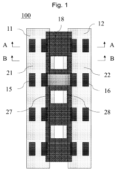
- The design incorporates alternating cells with specific well regions, source regions, and contact layers, including ohmic and Schottky contacts, to reduce channel density, enhance short-circuit tolerance, and minimize reverse leakage current and forward voltage drop, while maintaining the transistor's size and functionality.
Silicon carbide field-effect transistors
PatentActiveUS20220013661A1
Innovation
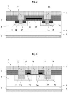
- A silicon carbide (SiC) metal-oxide-semiconductor field-effect transistor (MOSFET) design incorporating a substrate, drift region, spreading layer, body region, and source region with a gate structure that includes a gate oxide layer, aluminum nitride, and p-type gallium nitride layers, achieving low on-state specific resistance and high threshold voltage.
Thermal Management Strategies for SiC Devices
Thermal management is a critical aspect of SiC MOSFET reliability and performance, particularly when conducting failure analysis using advanced diagnostics. SiC devices operate at significantly higher temperatures than traditional silicon counterparts, with junction temperatures reaching up to 200°C compared to silicon's typical 150°C limit. This thermal advantage, while beneficial for power density, creates unique challenges for heat dissipation and thermal management strategies.
The thermal conductivity of SiC (approximately 3.7 W/cm·K) exceeds that of silicon, yet the higher power densities and switching frequencies of SiC MOSFETs generate substantial heat that must be effectively managed. Advanced cooling solutions including direct liquid cooling, double-sided cooling, and phase-change materials have emerged as promising approaches for SiC thermal management. These solutions can reduce thermal resistance by 30-50% compared to conventional air cooling methods.
When performing failure analysis diagnostics, thermal imaging techniques such as infrared thermography and liquid crystal thermography provide crucial insights into device temperature distribution. These methods can detect hotspots that often precede catastrophic failures, with modern systems capable of microsecond-level temporal resolution and sub-micron spatial resolution.
Dynamic thermal impedance measurements represent another valuable diagnostic tool, allowing for the identification of degradation in die-attach materials and thermal interfaces. Research indicates that up to 60% of SiC MOSFET failures can be attributed to packaging-related thermal issues rather than the semiconductor itself, highlighting the importance of comprehensive thermal analysis in failure investigations.
Advanced thermal simulation tools incorporating multi-physics modeling have become essential for predicting thermal behavior under various operating conditions. These simulations can accurately forecast temperature distributions within 5% of measured values when properly calibrated, enabling more effective failure analysis and preventive measures.
Emerging technologies such as embedded cooling channels and advanced thermal interface materials (TIMs) with thermal conductivities exceeding 25 W/m·K are showing promise for next-generation SiC devices. These innovations may reduce junction-to-case thermal resistance by up to 40%, significantly enhancing reliability and performance under extreme operating conditions.
For comprehensive failure analysis, correlation between thermal behavior and electrical parameters is essential. Advanced diagnostics increasingly employ simultaneous thermal and electrical measurements to establish causal relationships between thermal events and electrical failures, providing a more complete picture of failure mechanisms in SiC MOSFETs.
Standardization Efforts in SiC Failure Analysis
The standardization of SiC MOSFET failure analysis methodologies represents a critical frontier in the wide bandgap semiconductor industry. Currently, several international organizations are actively developing comprehensive standards to address the unique challenges posed by SiC technology. The JEDEC JC-70 committee has established dedicated working groups focused on reliability assessment and failure analysis protocols specifically for SiC power devices, with particular emphasis on standardizing test conditions that accurately reflect the thermal and electrical stress environments these devices encounter in real-world applications.
IEEE has similarly contributed through its P2907 initiative, which aims to create uniform testing procedures for SiC MOSFET gate oxide reliability—a critical failure point identified across multiple device generations. This standard addresses threshold voltage instability measurement techniques and accelerated lifetime testing parameters that are essential for predicting long-term device performance.
Industry consortia such as PowerAmerica and the European ECPE have established collaborative platforms where manufacturers, academic institutions, and end-users jointly develop best practices for failure analysis. These efforts have resulted in shared databases of failure signatures and corresponding root causes, significantly accelerating the diagnostic process across the industry.
A notable advancement in standardization has been the development of the SiC-FA protocol, which outlines a systematic approach to failure analysis beginning with non-destructive techniques before progressing to more invasive methods. This protocol emphasizes the preservation of failure evidence through carefully sequenced analytical steps, addressing the unique challenges of SiC material systems where traditional silicon-based approaches often prove inadequate.
The automotive industry, through the Automotive Electronics Council (AEC), has been particularly active in developing SiC-specific qualification standards that incorporate failure analysis methodologies suitable for the demanding reliability requirements of vehicle electrification. AEC-Q101 revisions now include specific provisions for SiC MOSFET qualification with standardized failure analysis reporting requirements.
Challenges to standardization efforts include the rapid evolution of SiC device technologies, variations in manufacturing processes between suppliers, and the proprietary nature of certain failure mechanisms. Despite these obstacles, consensus is emerging around key analytical techniques such as photon emission microscopy protocols optimized for SiC's wider bandgap, standardized sample preparation methods for electron microscopy that preserve the integrity of failure sites, and electrical characterization sequences that effectively isolate failure modes unique to SiC technology.
Unlock deeper insights with Patsnap Eureka Quick Research — get a full tech report to explore trends and direct your research. Try now!
Generate Your Research Report Instantly with AI Agent
Supercharge your innovation with Patsnap Eureka AI Agent Platform!