Silicon Carbide Wafer Coating Properties in Semiconductors
OCT 14, 20259 MIN READ
Generate Your Research Report Instantly with AI Agent
Patsnap Eureka helps you evaluate technical feasibility & market potential.
SiC Wafer Coating Evolution and Objectives
Silicon carbide (SiC) wafer coating technology has evolved significantly over the past four decades, transforming from experimental applications to a cornerstone of modern high-power and high-frequency semiconductor devices. The journey began in the 1980s with rudimentary coating techniques that suffered from high defect densities and poor uniformity. By the 1990s, researchers had developed chemical vapor deposition (CVD) methods specifically tailored for SiC substrates, marking a critical advancement in coating quality.
The early 2000s witnessed a paradigm shift with the introduction of atomic layer deposition (ALD) techniques for SiC wafers, enabling unprecedented control over coating thickness and composition at the atomic scale. This period also saw the first commercial applications of SiC-based power devices, primarily in niche industrial markets where traditional silicon solutions were inadequate.
Between 2010 and 2020, significant improvements in epitaxial growth processes reduced defect densities by over two orders of magnitude, while simultaneously increasing wafer diameters from 2 inches to 6 inches. These advancements dramatically reduced production costs and expanded the commercial viability of SiC-based semiconductors across multiple industries.
Current coating technologies focus on enhancing three critical properties: thermal stability at extreme temperatures (>600°C), interface quality between SiC and dielectric materials, and long-term reliability under high electric field conditions. Recent innovations include stress-engineered coatings that minimize lattice mismatch issues and novel passivation techniques that reduce interface trap densities by more than 90% compared to early 2000s standards.
The primary technical objectives for SiC wafer coating development center around overcoming persistent challenges in the semiconductor industry. These include reducing micropipe defects to below 0.1 cm^-2, achieving uniform coatings across larger diameter wafers (8-inch and beyond), and developing cost-effective methods for high-volume manufacturing without compromising quality.
Looking forward, the technology roadmap aims to enable SiC semiconductors to operate reliably at junction temperatures exceeding 300°C, withstand breakdown fields above 10 MV/cm, and maintain stable performance under radiation exposure for aerospace and nuclear applications. Additionally, there is growing emphasis on environmentally sustainable coating processes that reduce hazardous chemical usage and energy consumption.
The convergence of these technological advancements is expected to position SiC as the material of choice for next-generation power electronics in electric vehicles, renewable energy systems, and 5G/6G infrastructure, where efficiency, size, and reliability demands cannot be met by conventional silicon technology.
Market Demand Analysis for SiC Semiconductor Coatings
The global market for Silicon Carbide (SiC) semiconductor coatings has experienced remarkable growth in recent years, primarily driven by the increasing demand for high-performance electronic devices across various industries. The compound annual growth rate (CAGR) for SiC-based semiconductors is projected to exceed 25% through 2028, significantly outpacing traditional silicon semiconductor growth rates.
Power electronics represents the largest application segment for SiC semiconductor coatings, accounting for approximately 60% of the total market share. This dominance stems from SiC's superior properties in high-voltage, high-temperature, and high-frequency applications. The automotive sector, particularly electric vehicles (EVs), has emerged as the fastest-growing end-user segment, with major manufacturers increasingly adopting SiC-based power modules for inverters and on-board chargers.
The industrial sector constitutes another substantial market for SiC semiconductor coatings, with applications in motor drives, power supplies, and renewable energy systems. The renewable energy market, especially solar inverters and wind power converters, has shown strong adoption rates due to SiC's ability to improve energy conversion efficiency by 2-3% compared to traditional silicon-based solutions.
Regional analysis reveals that Asia-Pacific currently dominates the market with over 45% share, led by China, Japan, and South Korea. These countries have established robust manufacturing ecosystems and government initiatives supporting wide bandgap semiconductor development. North America and Europe follow with significant market shares, driven by automotive and industrial applications respectively.
Market forecasts indicate that the SiC coating materials segment will grow at an accelerated pace, with specialized coatings designed to enhance thermal management and reduce interface defects gaining particular traction. The demand for high-quality protective and functional coatings for SiC wafers is expected to increase as device manufacturers push for higher reliability and longer operational lifetimes.
Customer requirements are evolving toward coatings that can withstand increasingly extreme operating conditions while maintaining electrical performance. Specifically, there is growing demand for coatings that can operate reliably at junction temperatures above 200°C, withstand voltage ratings exceeding 1200V, and provide enhanced protection against environmental factors.
Supply chain analysis reveals potential bottlenecks in high-purity coating materials and specialized deposition equipment, which could impact market growth. Several key suppliers have announced capacity expansion plans to address these constraints, though qualification timelines for new materials remain lengthy in semiconductor applications.
Global SiC Coating Technology Status and Challenges
Silicon carbide (SiC) coating technology has witnessed significant advancements globally, yet faces numerous challenges that impede its widespread adoption in semiconductor applications. Currently, the global landscape of SiC coating technology demonstrates varying levels of maturity across different regions, with North America, Europe, and East Asia emerging as primary innovation hubs.
In North America, companies like Wolfspeed, II-VI Incorporated, and GT Advanced Technologies have established robust SiC coating capabilities, focusing primarily on chemical vapor deposition (CVD) and atomic layer deposition (ALD) techniques. These organizations have successfully commercialized several coating solutions that enhance the thermal stability and electrical properties of SiC wafers.
European research institutions and companies, particularly in Germany and France, have made substantial contributions to SiC coating technology development. Organizations such as Fraunhofer Institute and STMicroelectronics have pioneered advanced plasma-enhanced chemical vapor deposition (PECVD) methods that improve coating uniformity and adhesion properties.
The Asia-Pacific region, led by Japan and South Korea, has demonstrated remarkable progress in developing cost-effective SiC coating solutions. Companies like ROHM Semiconductor and Showa Denko have invested heavily in optimizing physical vapor deposition (PVD) techniques for large-diameter SiC wafers.
Despite these advancements, several critical challenges persist in SiC coating technology. The foremost challenge involves achieving uniform coating thickness across large-diameter wafers (6-inch and above), which is essential for maintaining consistent electrical properties. Current technologies struggle to deliver the nanometer-level precision required for advanced semiconductor applications.
Another significant obstacle is the high-temperature requirements for most SiC coating processes, typically exceeding 1000°C. These extreme conditions can induce thermal stress, leading to wafer warping and defect formation. Developing lower-temperature coating processes without compromising quality remains a formidable challenge.
Interface quality between the SiC substrate and coating layers presents another technical hurdle. Achieving atomically smooth interfaces with minimal defects is crucial for optimal device performance but remains difficult to accomplish consistently at production scales.
Cost factors also significantly constrain global SiC coating technology advancement. The high capital expenditure for specialized equipment and the operational expenses associated with precise process control make SiC coating economically challenging for many potential adopters.
Environmental considerations pose additional challenges, as traditional SiC coating processes often utilize hazardous precursor materials and generate significant waste. Developing greener alternatives while maintaining performance specifications represents an emerging focus area for research institutions worldwide.
Current SiC Wafer Coating Methodologies
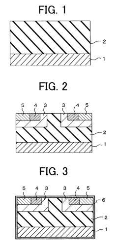
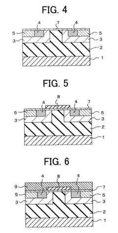
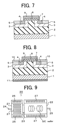
01 Protective coating materials for SiC wafers
Various materials can be applied as protective coatings on silicon carbide wafers to enhance their properties. These include oxide layers, nitride films, and metal-based coatings that provide protection against environmental factors, chemical reactions, and mechanical damage. These coatings can significantly improve the durability and performance of SiC wafers in high-temperature and harsh environments while maintaining the semiconductor properties of the substrate.- Protective coating materials for SiC wafers: Various materials can be used as protective coatings for silicon carbide wafers to enhance their properties and durability. These include oxide layers, nitride films, and metal-based coatings that provide protection against environmental factors and processing conditions. These coatings help to preserve the integrity of the SiC wafer surface while maintaining or enhancing its electrical and thermal properties.
- Coating methods for silicon carbide substrates: Different deposition techniques can be employed to apply coatings on silicon carbide wafers, including chemical vapor deposition (CVD), physical vapor deposition (PVD), atomic layer deposition (ALD), and epitaxial growth. These methods allow for precise control of coating thickness, uniformity, and composition, which are critical for achieving desired properties such as electrical conductivity, thermal stability, and mechanical strength.
- Thermal and electrical properties of coated SiC wafers: Coatings on silicon carbide wafers can significantly influence their thermal and electrical properties. Properly designed coatings can enhance heat dissipation, improve electrical conductivity or insulation (depending on the application requirements), and optimize the performance of SiC-based electronic devices. These properties are particularly important for high-power and high-temperature applications where silicon carbide excels.
- Surface modification and interface properties: Surface treatments and modifications of silicon carbide wafers before or during coating processes can significantly affect the adhesion, uniformity, and overall quality of the coating. Techniques such as plasma treatment, chemical etching, and thermal annealing can be used to optimize the interface between the SiC substrate and the coating layer, reducing defects and enhancing the coating's functional properties.
- Advanced coatings for specialized applications: Specialized coatings for silicon carbide wafers have been developed for specific applications such as power electronics, MEMS devices, and sensors. These advanced coatings may incorporate multiple layers, nanostructures, or functional materials to achieve specific performance characteristics such as enhanced breakdown voltage, reduced interface states, improved radiation hardness, or selective chemical resistance.
02 Deposition techniques for SiC wafer coatings
Multiple deposition methods are employed to create high-quality coatings on silicon carbide wafers. These techniques include chemical vapor deposition (CVD), atomic layer deposition (ALD), physical vapor deposition (PVD), and epitaxial growth processes. Each method offers specific advantages in terms of coating uniformity, thickness control, and adhesion properties, allowing for customized coating solutions based on the intended application of the SiC wafer.Expand Specific Solutions03 Thermal and electrical properties of coated SiC wafers
Coatings applied to silicon carbide wafers can significantly modify their thermal and electrical characteristics. Specialized coatings can enhance thermal conductivity, improve heat dissipation, and provide better electrical insulation or conductivity depending on the application requirements. These modified properties make coated SiC wafers particularly valuable in high-power electronics, high-temperature applications, and devices operating under extreme conditions.Expand Specific Solutions04 Surface modification and interface engineering
Surface treatments and interface engineering techniques are crucial for optimizing the properties of coated silicon carbide wafers. These processes include surface activation, passivation treatments, and the creation of transition layers to improve coating adhesion and reduce interface defects. Properly engineered interfaces between the SiC substrate and coating layers can minimize stress, prevent delamination, and enhance overall device performance and reliability.Expand Specific Solutions05 Advanced functional coatings for specialized applications
Innovative functional coatings for silicon carbide wafers are being developed for specialized applications. These include optically transparent coatings for sensor applications, biocompatible coatings for medical devices, and chemically resistant coatings for harsh environment operations. Additionally, multi-layer coating systems can provide combinations of properties such as wear resistance, corrosion protection, and enhanced electrical performance, expanding the range of applications for SiC-based devices.Expand Specific Solutions
Key Industry Players in SiC Semiconductor Coatings
The Silicon Carbide (SiC) wafer coating market is currently in a growth phase, with increasing adoption across semiconductor applications due to SiC's superior thermal conductivity and electrical properties. The global market size is projected to expand significantly, driven by demand in electric vehicles, power electronics, and renewable energy sectors. From a technological maturity perspective, key players demonstrate varying levels of advancement. Wolfspeed has established itself as a market leader with extensive SiC expertise, while RESONAC and Sumitomo Electric are developing specialized coating technologies. STMicroelectronics, Toshiba, and Fuji Electric are leveraging their semiconductor manufacturing capabilities to enhance SiC wafer coating properties. Chinese companies like BYD and Huawei are rapidly investing in this technology to secure supply chain independence. Research collaborations between industry leaders and institutions such as University of Warwick and Northwestern Polytechnical University are accelerating innovation in coating methodologies.
Wolfspeed, Inc.
Technical Solution: Wolfspeed has pioneered advanced epitaxial coating techniques for Silicon Carbide (SiC) wafers, utilizing Chemical Vapor Deposition (CVD) to create ultra-pure SiC epitaxial layers with controlled doping profiles. Their proprietary process achieves defect densities below 1 per cm², significantly lower than industry averages. Wolfspeed's 150mm and 200mm SiC wafer coating technology incorporates a multi-zone hot-wall CVD reactor system that ensures uniform temperature distribution across the wafer surface, resulting in thickness variations of less than ±2%. Their coating process includes in-situ surface preparation steps that remove subsurface damage before epitaxial growth, enhancing crystal quality and electrical performance. Wolfspeed has also developed specialized passivation layers that reduce interface states and improve long-term reliability of SiC power devices, particularly important for high-temperature and high-voltage applications.
Strengths: Industry-leading epitaxial quality with minimal defect density; excellent thickness uniformity across large-diameter wafers; superior high-temperature performance of coatings. Weaknesses: Higher production costs compared to silicon alternatives; limited production capacity despite recent expansions; longer processing times for high-quality epitaxial layers.
Sumitomo Electric Industries Ltd.
Technical Solution: Sumitomo Electric has developed a proprietary High-Temperature Chemical Vapor Deposition (HT-CVD) process for SiC wafer coating that operates at temperatures exceeding 1600°C. This approach enables the formation of exceptionally high-quality epitaxial layers with carrier mobility values approaching theoretical limits. Their coating technology incorporates a unique gas flow management system that minimizes silicon droplet formation during deposition, a common challenge in SiC epitaxy. Sumitomo's process achieves doping concentration uniformity of ±5% across 150mm wafers, supporting the production of high-voltage (>10kV) power devices. The company has also pioneered multi-layer epitaxial structures with precisely controlled transition regions between layers of different doping concentrations, essential for next-generation trench MOSFET devices. Their coating technology includes specialized surface treatments that reduce basal plane dislocations by approximately 60% compared to untreated substrates.
Strengths: Exceptional epitaxial quality with near-theoretical carrier mobility; excellent doping control and uniformity; advanced multi-layer capabilities for complex device structures. Weaknesses: Extremely high process temperatures increase manufacturing costs and equipment wear; limited to smaller diameter wafers compared to some competitors; higher energy consumption in production.
Critical Patents and Innovations in SiC Coating Technology
Method of manufacturing silicon carbide semiconductor device
PatentActiveUS7820534B2
Innovation
- A method involving the formation of a high-purity carbon protection film over the entire surface of a silicon carbide wafer using a chemical vapor deposition method with a hydrocarbon gas, which prevents evaporation and thermal stress, thereby reducing step bunching and contamination.
Susceptor and method for manufacturing the same
PatentWO2020051217A1
Innovation
- A susceptor with a structured surface comprising a graphite substrate coated with silicon carbide (SiC), featuring a convex or concave design with parallel placing elements of equal height, and a surrounding groove for improved heat transfer and mechanical stability, reducing thermal stress and warping.

Environmental Impact of SiC Coating Processes
The manufacturing processes for Silicon Carbide (SiC) wafer coatings in semiconductor applications present significant environmental considerations that must be addressed as this technology continues to expand. Traditional SiC coating methods, particularly Chemical Vapor Deposition (CVD), consume substantial energy due to the high temperatures (1200-1600°C) required for proper crystallization and adhesion. This energy-intensive process contributes considerably to the carbon footprint of semiconductor manufacturing facilities, with estimates suggesting that coating operations can account for up to 15-20% of a fab's total energy consumption.
Water usage represents another critical environmental concern. The cleaning and preparation phases of SiC wafer coating typically require 5-7 gallons of ultra-pure water per wafer, creating substantial water demand in regions where semiconductor manufacturing is concentrated. This becomes particularly problematic in water-stressed areas such as Arizona, Taiwan, and parts of China where many semiconductor facilities operate.
Chemical waste management presents ongoing challenges for the industry. SiC coating processes utilize precursor gases including silane (SiH4) and various carbon-containing compounds that are both toxic and potentially hazardous. Unreacted precursors and byproducts must undergo specialized treatment before disposal, adding complexity and cost to waste management systems. Recent industry data indicates that for every square meter of coated wafer surface, approximately 0.5-1.2 kg of chemical waste is generated.
Air emissions from SiC coating operations contain volatile organic compounds (VOCs), particulate matter, and greenhouse gases that require abatement systems. While modern facilities typically employ thermal oxidizers and scrubbers that can achieve 95-99% reduction in harmful emissions, the remaining output still contributes to local air quality concerns and global climate impacts.
Emerging technologies show promise for reducing these environmental impacts. Atomic Layer Deposition (ALD) techniques for SiC coating can operate at lower temperatures (300-600°C) and demonstrate up to 40% reduction in precursor gas usage compared to traditional CVD methods. Additionally, closed-loop water recycling systems implemented by leading manufacturers have demonstrated potential to reduce water consumption by 60-80%, though these systems require significant capital investment.
Regulatory frameworks governing SiC coating processes continue to evolve globally, with the European Union's REACH regulations and similar initiatives in Japan and South Korea imposing increasingly stringent requirements on chemical usage and emissions. Companies investing in SiC technology must factor these environmental compliance costs into their strategic planning, as they represent a growing proportion of operational expenses in advanced semiconductor manufacturing.
Quality Control Standards for SiC Wafer Coatings
Quality control standards for Silicon Carbide (SiC) wafer coatings have evolved significantly to meet the demanding requirements of modern semiconductor applications. These standards encompass multiple dimensions of coating integrity, including thickness uniformity, defect density, adhesion strength, and chemical purity. Industry benchmarks typically require coating thickness variations to remain below ±2% across the wafer surface, with defect densities not exceeding 0.1 defects/cm² for particles larger than 0.3μm.
The International Semiconductor Manufacturing Standards (ISMS) has established comprehensive protocols for SiC coating evaluation, mandating rigorous testing procedures including four-point probe measurements, ellipsometry, and X-ray reflectometry for thickness verification. Surface quality assessment standards require scanning electron microscopy (SEM) and atomic force microscopy (AFM) analyses to detect nanoscale imperfections that could compromise device performance.
Thermal stability testing has become increasingly stringent, with requirements for coatings to maintain structural integrity through temperature cycling from -65°C to 600°C without delamination or cracking. This reflects the growing application of SiC in high-temperature and high-power electronics environments where thermal management is critical.
Electrical property standards have also tightened, with specifications for breakdown voltage typically exceeding 2.5 MV/cm and leakage current densities below 10⁻⁸ A/cm² at rated voltage. These parameters ensure reliable operation in power electronics applications where SiC offers significant advantages over traditional silicon.
Chemical resistance testing protocols now include exposure to aggressive environments including hydrofluoric acid, potassium hydroxide, and various plasma chemistries used in subsequent processing steps. Coatings must demonstrate less than 1% degradation in thickness or surface roughness after standardized chemical exposure tests.
In-line monitoring has become standard practice, with automated optical inspection systems calibrated to detect coating anomalies as small as 0.1μm. Statistical process control methods, including cumulative sum (CUSUM) and exponentially weighted moving average (EWMA) charts, are widely implemented to track coating quality trends and enable early intervention when processes drift toward control limits.
Certification requirements now often include documentation of coating material purity (99.9999% minimum for critical applications), process repeatability metrics, and comprehensive traceability of materials throughout the supply chain. Third-party verification through organizations like SEMI (Semiconductor Equipment and Materials International) has become increasingly common for manufacturers seeking to establish credibility in the competitive SiC market.
Unlock deeper insights with Patsnap Eureka Quick Research — get a full tech report to explore trends and direct your research. Try now!
Generate Your Research Report Instantly with AI Agent
Supercharge your innovation with Patsnap Eureka AI Agent Platform!