Silicon Carbide Wafer Compliance with Industry Regulations
OCT 14, 202510 MIN READ
Generate Your Research Report Instantly with AI Agent
Patsnap Eureka helps you evaluate technical feasibility & market potential.
SiC Wafer Technology Background and Objectives
Silicon carbide (SiC) wafer technology represents a significant advancement in semiconductor materials, evolving from its initial discovery in 1824 by Jöns Jacob Berzelius to becoming a cornerstone material for high-power, high-frequency, and high-temperature electronic applications. The progression of SiC wafer technology has been marked by continuous improvements in crystal growth techniques, defect reduction, and wafer size expansion, moving from small diameter prototypes to commercially viable 6-inch and now emerging 8-inch wafers.
The fundamental advantage of SiC lies in its superior material properties compared to traditional silicon. With a bandgap nearly three times wider than silicon (3.2 eV vs 1.1 eV), SiC demonstrates exceptional thermal conductivity (3-4 times higher), breakdown electric field strength (10 times greater), and saturated electron drift velocity (twice as fast). These properties enable devices that can operate at temperatures exceeding 600°C, withstand voltage stresses up to 10 times higher than silicon-based counterparts, and function at significantly higher frequencies with reduced switching losses.
Industry regulations governing SiC wafer production have evolved alongside technological advancements, with standards bodies such as SEMI, JEDEC, and ISO establishing increasingly stringent specifications for material quality, dimensional tolerances, and contamination control. The primary objective in this technological domain is achieving full compliance with these regulations while simultaneously improving yield rates and reducing production costs to enable broader market adoption.
Current regulatory frameworks focus on several critical aspects: crystalline quality metrics (micropipe density, dislocation density, and polytype uniformity), surface quality parameters (roughness, flatness, and bow/warp), electrical characteristics (resistivity uniformity and carrier lifetime), and contamination control (metallic and particulate impurities). Meeting these standards requires sophisticated manufacturing processes and advanced metrology capabilities.
The technological trajectory aims to address persistent challenges in SiC wafer production, particularly the reduction of crystal defects that impact device performance and reliability. Research efforts are concentrated on developing improved crystal growth techniques, post-growth processing methods, and defect characterization tools that align with evolving regulatory requirements.
Looking forward, the industry anticipates regulatory frameworks to become increasingly comprehensive, potentially incorporating sustainability metrics, lifecycle assessment parameters, and expanded performance specifications as SiC applications diversify into automotive, renewable energy, and industrial sectors. The technological objective is thus twofold: achieving full compliance with current regulations while developing manufacturing capabilities that can anticipate and adapt to future regulatory developments.
Market Demand Analysis for SiC Wafers
The Silicon Carbide (SiC) wafer market is experiencing unprecedented growth driven primarily by the rapid expansion of electric vehicles (EVs) and renewable energy sectors. Current market assessments indicate that the global SiC wafer market reached approximately $1.2 billion in 2022 and is projected to grow at a compound annual growth rate of 18-20% through 2030, potentially reaching $5 billion by the end of the decade. This remarkable growth trajectory is underpinned by SiC's superior material properties that enable high-temperature, high-frequency, and high-voltage applications.
The automotive sector represents the largest demand driver, accounting for nearly 60% of the total SiC wafer market. As automotive manufacturers increasingly transition to electric powertrains, the demand for SiC-based power electronics has surged due to their ability to increase vehicle range, reduce charging times, and improve overall system efficiency. Major automotive OEMs have announced plans to incorporate SiC technology in their upcoming EV models, signaling sustained demand growth.
Industrial power systems constitute the second-largest market segment, representing approximately 20% of current demand. The push toward energy efficiency in manufacturing processes and industrial automation has accelerated adoption of SiC-based power conversion systems. Additionally, the renewable energy sector, particularly solar inverters and wind power systems, has emerged as a significant growth market, currently accounting for 15% of SiC wafer demand with projections indicating faster growth than other segments.
Geographically, Asia-Pacific dominates the market with approximately 45% share, followed by North America (30%) and Europe (20%). China has made significant investments in developing domestic SiC wafer manufacturing capabilities as part of its strategic focus on semiconductor self-sufficiency, while Japan maintains leadership in high-quality wafer production for automotive applications.
A critical market dynamic is the persistent supply-demand imbalance. Despite capacity expansions announced by major manufacturers, industry analysts predict a supply shortage continuing through at least 2025, particularly for larger diameter wafers (6-inch and 8-inch) that comply with stringent automotive and industrial quality standards. This shortage has maintained price premiums for regulation-compliant SiC wafers, with automotive-grade wafers commanding 15-25% higher prices than standard grades.
Customer requirements are increasingly focused on wafer quality consistency, defect density reduction, and compliance with industry-specific regulations such as IATF 16949 for automotive applications and various regional environmental standards. The market is witnessing a shift toward larger diameter wafers (transitioning from 4-inch to 6-inch and 8-inch) to improve economies of scale and reduce overall device costs, though this transition presents additional compliance challenges.
Current Regulatory Landscape and Technical Challenges
The global regulatory landscape for Silicon Carbide (SiC) wafers is increasingly complex, with standards varying significantly across regions. In the United States, the Semiconductor Industry Association (SIA) has established specific guidelines for SiC wafer manufacturing, focusing on material purity, crystalline structure integrity, and surface defect tolerances. The European Union, through its Restriction of Hazardous Substances (RoHS) and Registration, Evaluation, Authorization and Restriction of Chemicals (REACH) regulations, imposes strict controls on chemical processes used in SiC wafer production, particularly regarding heavy metal contamination and waste management.
Japan's Ministry of Economy, Trade and Industry (METI) has implemented the most stringent quality standards for SiC wafers, requiring 99.9995% purity for power electronics applications. China, meanwhile, has recently updated its GB/T standards for semiconductor materials, introducing new specifications for SiC wafer thickness uniformity and electrical characteristics that manufacturers must meet to access the rapidly growing Chinese market.
Technical challenges in meeting these diverse regulations are substantial. The primary difficulty lies in achieving consistent micropipe density reduction across large-diameter wafers. Current industry leaders struggle to maintain defect densities below 1 cm² for 6-inch wafers, with the challenge multiplying for the emerging 8-inch wafer technology. This creates significant yield issues when attempting to meet Japanese and European specifications simultaneously.
Surface contamination control presents another major hurdle. The detection and elimination of metallic impurities at the parts-per-trillion level required by advanced regulations necessitates clean room environments exceeding Class 10 standards and specialized metrology equipment that few manufacturers currently possess. The capital expenditure required for such facilities often exceeds $100 million, creating a significant barrier to entry for smaller manufacturers.
Crystal polytypes management remains problematic, with regulations increasingly distinguishing between 4H-SiC and 6H-SiC requirements. The industry currently lacks standardized methods to consistently produce specific polytypes at scale while maintaining the required electrical properties, particularly the high breakdown voltage characteristics demanded by automotive applications under both EU and US regulations.
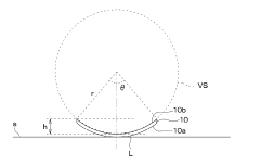
Wafer bow and warp specifications have become increasingly stringent, with tolerances now below 10 μm for 6-inch wafers in premium applications. Meeting these specifications while simultaneously addressing other parameters creates complex engineering trade-offs that often require complete redesign of manufacturing processes, particularly challenging for facilities originally designed for silicon wafer production.
The regulatory divergence between regions creates additional compliance complexity, with manufacturers often forced to implement separate production lines or extensive sorting procedures to meet different market requirements, significantly impacting production economics and global supply chain efficiency.
Japan's Ministry of Economy, Trade and Industry (METI) has implemented the most stringent quality standards for SiC wafers, requiring 99.9995% purity for power electronics applications. China, meanwhile, has recently updated its GB/T standards for semiconductor materials, introducing new specifications for SiC wafer thickness uniformity and electrical characteristics that manufacturers must meet to access the rapidly growing Chinese market.
Technical challenges in meeting these diverse regulations are substantial. The primary difficulty lies in achieving consistent micropipe density reduction across large-diameter wafers. Current industry leaders struggle to maintain defect densities below 1 cm² for 6-inch wafers, with the challenge multiplying for the emerging 8-inch wafer technology. This creates significant yield issues when attempting to meet Japanese and European specifications simultaneously.
Surface contamination control presents another major hurdle. The detection and elimination of metallic impurities at the parts-per-trillion level required by advanced regulations necessitates clean room environments exceeding Class 10 standards and specialized metrology equipment that few manufacturers currently possess. The capital expenditure required for such facilities often exceeds $100 million, creating a significant barrier to entry for smaller manufacturers.
Crystal polytypes management remains problematic, with regulations increasingly distinguishing between 4H-SiC and 6H-SiC requirements. The industry currently lacks standardized methods to consistently produce specific polytypes at scale while maintaining the required electrical properties, particularly the high breakdown voltage characteristics demanded by automotive applications under both EU and US regulations.
Wafer bow and warp specifications have become increasingly stringent, with tolerances now below 10 μm for 6-inch wafers in premium applications. Meeting these specifications while simultaneously addressing other parameters creates complex engineering trade-offs that often require complete redesign of manufacturing processes, particularly challenging for facilities originally designed for silicon wafer production.
The regulatory divergence between regions creates additional compliance complexity, with manufacturers often forced to implement separate production lines or extensive sorting procedures to meet different market requirements, significantly impacting production economics and global supply chain efficiency.
Current Compliance Solutions and Methodologies
01 Silicon carbide wafer manufacturing compliance standards
Silicon carbide wafer manufacturing involves specific compliance standards to ensure quality and performance. These standards address crystal growth, surface preparation, and defect control. Manufacturers must adhere to industry specifications regarding wafer thickness uniformity, surface roughness, and crystalline quality. Compliance with these standards is essential for producing SiC wafers suitable for high-performance semiconductor applications, particularly in power electronics and high-temperature environments.- Silicon carbide wafer manufacturing processes: Various manufacturing processes are employed to produce silicon carbide wafers with improved compliance characteristics. These processes include specific growth techniques, cutting methods, and surface treatments that enhance the wafer's mechanical properties and reduce defects. Advanced manufacturing techniques help to control wafer bow, warp, and other dimensional parameters that are critical for compliance with industry standards.
- Wafer surface treatment and polishing techniques: Surface treatment and polishing techniques are essential for achieving compliant silicon carbide wafers. These techniques include chemical-mechanical polishing, plasma etching, and thermal treatments that reduce surface roughness and remove subsurface damage. Properly treated wafer surfaces ensure better device performance and reliability, while meeting stringent compliance requirements for semiconductor applications.
- Defect detection and quality control methods: Advanced defect detection and quality control methods are implemented to ensure silicon carbide wafers meet compliance standards. These include optical inspection, X-ray topography, and electrical characterization techniques that identify and quantify various defects such as micropipes, dislocations, and stacking faults. Comprehensive quality control processes help maintain consistent wafer properties and ensure compliance with industry specifications.
- Substrate engineering for improved compliance: Engineering the substrate structure of silicon carbide wafers can significantly improve their compliance characteristics. This includes techniques such as epitaxial growth optimization, buffer layer implementation, and controlled doping profiles. These approaches help manage internal stresses, improve crystal quality, and enhance the overall mechanical stability of the wafers, leading to better compliance with device manufacturing requirements.
- Compliance testing and standardization: Standardized testing protocols and compliance verification methods are crucial for silicon carbide wafer qualification. These include mechanical testing for bow and warp, electrical characterization for resistivity uniformity, and dimensional measurements for thickness variation. Industry standards and specifications provide benchmarks for wafer compliance, ensuring that silicon carbide wafers meet the requirements for advanced semiconductor applications.
02 Mechanical compliance in SiC wafer handling and processing
Mechanical compliance is critical in silicon carbide wafer handling and processing due to the material's inherent brittleness and hardness. Specialized handling equipment and techniques are required to prevent wafer breakage and damage during manufacturing processes. Compliance mechanisms in wafer carriers, chucks, and transfer systems must accommodate the unique physical properties of SiC while maintaining precise positioning. These mechanical compliance solutions help minimize stress-induced defects and improve overall yield in SiC wafer production.Expand Specific Solutions03 Thermal compliance considerations for SiC wafers
Thermal compliance is a significant factor in silicon carbide wafer processing due to the material's high thermal conductivity and stability. Temperature management systems must comply with specific thermal profiles to prevent wafer warpage and stress during high-temperature processes like epitaxial growth and annealing. Thermal compliance solutions include specialized heating elements, temperature controllers, and thermal isolation techniques that accommodate SiC's unique thermal expansion characteristics while maintaining process uniformity across the wafer surface.Expand Specific Solutions04 Regulatory and environmental compliance for SiC wafer production
Silicon carbide wafer production must adhere to various regulatory and environmental compliance requirements. These include handling of hazardous materials, waste management protocols, and emissions control during manufacturing processes. Facilities producing SiC wafers must comply with local and international regulations regarding chemical usage, worker safety, and environmental impact. Sustainable manufacturing practices are increasingly important for compliance, including energy efficiency measures and reduced use of environmentally harmful substances in the production of high-quality silicon carbide wafers.Expand Specific Solutions05 Quality assurance and testing compliance for SiC wafers
Quality assurance and testing compliance are essential aspects of silicon carbide wafer production. This involves implementing standardized inspection protocols, defect characterization methods, and electrical performance testing. Compliance with quality standards requires sophisticated metrology equipment for measuring parameters such as micropipe density, surface roughness, and crystallographic orientation. Manufacturers must maintain detailed documentation of testing procedures and results to demonstrate compliance with customer specifications and industry standards, ensuring that SiC wafers meet the demanding requirements of advanced electronic applications.Expand Specific Solutions
Key Industry Players and Compliance Leaders
Silicon Carbide (SiC) wafer compliance with industry regulations is evolving in a rapidly growing market, currently transitioning from early adoption to mainstream implementation. The global SiC wafer market is expanding significantly, driven by electric vehicle adoption and renewable energy applications, with projections exceeding $2 billion by 2025. Leading players like Wolfspeed, STMicroelectronics, and SICC are advancing technological maturity through significant R&D investments, while GlobalWafers, SUMCO, and Siltronic bring established semiconductor manufacturing expertise. Companies such as RESONAC and TanKeBlue are focusing on specialized compliance solutions, particularly for automotive and power electronics applications. The regulatory landscape is becoming more structured as the technology matures, with companies increasingly prioritizing standardization to ensure cross-industry compatibility and safety compliance.
STMicroelectronics International NV
Technical Solution: STMicroelectronics has implemented a multi-tiered compliance strategy for their silicon carbide wafer production that addresses both regional and international regulatory requirements. Their approach centers on a proprietary Quality Management System specifically designed for wide bandgap semiconductor materials that integrates compliance requirements from ISO 9001, IATF 16949, and industry-specific standards. ST's compliance framework includes specialized testing protocols for SiC wafers that verify conformity with electrical performance parameters, mechanical specifications, and chemical purity levels required by various regulatory bodies. The company has developed an advanced material qualification process that includes accelerated stress testing, reliability modeling, and failure analysis to ensure their SiC wafers meet automotive-grade reliability standards (AEC-Q101) and power electronics requirements. ST has invested in automated inspection systems that utilize AI-enhanced optical and electrical testing to identify non-compliant wafers before they enter production streams[2]. Their regulatory compliance extends to environmental considerations with RoHS and REACH-compliant manufacturing processes and materials, supported by detailed documentation and certification processes that facilitate customer compliance requirements.
Strengths: Comprehensive integration of compliance requirements into manufacturing processes with strong focus on automotive-grade qualification. Advanced automated inspection systems provide high detection rates for non-compliant materials. Weaknesses: Complex compliance documentation requirements may increase administrative overhead and potentially impact production agility. Balancing regional regulatory variations across global manufacturing facilities creates consistency challenges.
SICC Co., Ltd.
Technical Solution: SICC has developed a specialized compliance framework for silicon carbide wafer production that focuses on meeting China's national standards while aligning with international requirements. Their approach includes a dual-certification strategy that ensures SiC wafers simultaneously comply with Chinese GB standards and international standards like SEMI and JEDEC. SICC implements a comprehensive material validation system that includes X-ray diffraction analysis, high-resolution transmission electron microscopy, and secondary ion mass spectrometry to verify crystal quality and impurity levels against regulatory thresholds. The company has established dedicated compliance testing laboratories equipped with advanced metrology tools that can detect non-conformities at the atomic level, ensuring their SiC wafers meet stringent purity requirements for semiconductor applications. SICC's regulatory compliance extends to production processes with automated documentation systems that generate material certificates and compliance declarations for each wafer lot[3]. Their traceability system incorporates blockchain technology to create immutable records of compliance testing results and material provenance, facilitating regulatory audits and customer verification processes. Additionally, SICC has implemented environmental compliance measures that address China's increasingly stringent emissions regulations while maintaining alignment with global environmental standards.
Strengths: Strong positioning for compliance with both Chinese national standards and international requirements provides competitive advantage in Asian markets. Advanced material characterization capabilities ensure high conformance rates with technical specifications. Weaknesses: Relatively newer entrant to global markets may have less established compliance history with some international regulatory bodies. Balancing domestic and international compliance requirements may create operational complexities.
Critical Patents and Technical Documentation Analysis
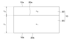
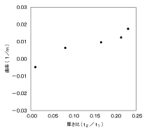
Silicon carbide wafer and manufacturing method of the same
PatentInactiveJP2023095359A
Innovation
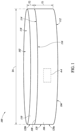
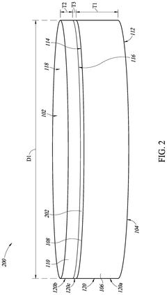
- Adjust the thickness ratio (t2/t1) and average impurity concentration ratio (n2/n1) of the epitaxial layer on the base wafer to control warpage without increasing surface roughness, using a SiC wafer with a base wafer doped with n-type impurities and an epitaxial layer also doped with n-type impurities.
Low resistivity polycrystalline based substrate or wafer
PatentPendingUS20240332365A1
Innovation
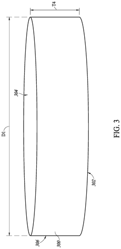
- A polycrystalline silicon carbide wafer with a resistivity of less than or equal to 2 mohm-cm and warpage of less than or equal to 75 μm is developed, coupled with a monocrystalline silicon carbide wafer using surface-activated bonding, reducing on-resistance and mechanical defects.
Environmental Impact and Sustainability Considerations
The manufacturing of Silicon Carbide (SiC) wafers presents significant environmental challenges that must be addressed to ensure sustainable industry growth. The production process requires substantial energy inputs, with temperatures exceeding 2000°C necessary for crystal growth. This energy-intensive nature contributes considerably to the carbon footprint of SiC wafer manufacturing, raising concerns about greenhouse gas emissions and climate impact. Industry leaders are increasingly implementing energy efficiency measures and exploring renewable energy sources to mitigate these effects.
Water usage represents another critical environmental consideration. The manufacturing process consumes large quantities of ultra-pure water for cleaning and processing steps. In regions facing water scarcity, this intensive consumption pattern raises sustainability concerns. Advanced water recycling systems and closed-loop water management approaches are being developed to reduce freshwater withdrawal and minimize wastewater discharge.
Chemical management poses additional environmental challenges. The production of SiC wafers involves various hazardous substances including acids, solvents, and dopants. These chemicals require careful handling, storage, and disposal to prevent environmental contamination. Leading manufacturers are adopting green chemistry principles, substituting hazardous substances with environmentally benign alternatives where technically feasible.
Waste management represents a growing focus area for regulatory compliance. The cutting, polishing, and processing of SiC wafers generates solid waste including silicon carbide particulates and slurry residues. These materials require proper disposal or recycling to minimize environmental impact. Innovative approaches to waste valorization are emerging, with some manufacturers developing processes to recover valuable materials from production waste streams.
Life cycle assessment (LCA) methodologies are increasingly being applied to SiC wafer production to quantify environmental impacts across the entire value chain. These assessments help identify hotspots for environmental improvement and support sustainability reporting. Industry regulations increasingly require comprehensive environmental impact assessments and mitigation strategies as part of compliance documentation.
The semiconductor industry is responding to these challenges through collaborative initiatives like the Responsible Business Alliance and the Semiconductor Climate Consortium. These organizations are developing industry-specific sustainability standards and best practices for SiC wafer manufacturing. Companies demonstrating environmental leadership are gaining competitive advantages through improved regulatory compliance, reduced operational costs, and enhanced brand reputation with environmentally conscious customers and investors.
Global Trade Regulations Affecting SiC Wafer Production
The global trade landscape for Silicon Carbide (SiC) wafers is increasingly complex, with regulations varying significantly across regions. Major semiconductor manufacturing nations such as the United States, Japan, European Union, and China have established distinct regulatory frameworks that directly impact SiC wafer production and distribution. These regulations encompass export controls, tariffs, quality standards, and environmental compliance requirements.
Export control regulations have become particularly stringent for SiC wafers due to their dual-use nature in both commercial and military applications. The U.S. Department of Commerce's Bureau of Industry and Security (BIS) has implemented specific controls on SiC materials under the Export Administration Regulations (EAR), requiring export licenses for shipments to certain countries. Similarly, the EU's dual-use regulation (Regulation 2021/821) places restrictions on SiC wafer exports to non-EU countries.
Tariff structures significantly influence the global SiC wafer supply chain. The U.S.-China trade tensions have resulted in increased tariffs on semiconductor materials, including SiC wafers, affecting pricing strategies and manufacturing location decisions. The Harmonized Tariff Schedule (HTS) classifications for SiC wafers vary between countries, creating compliance challenges for international manufacturers and distributors.
Environmental regulations also play a crucial role in SiC wafer production. The EU's Restriction of Hazardous Substances (RoHS) directive and Registration, Evaluation, Authorization, and Restriction of Chemicals (REACH) regulation impose strict requirements on materials used in semiconductor manufacturing. Similarly, Japan's Chemical Substances Control Law (CSCL) and China's Measures for Environmental Management of New Chemical Substances establish comparable frameworks in their respective regions.
Trade agreements have created both opportunities and challenges for SiC wafer manufacturers. The Comprehensive and Progressive Agreement for Trans-Pacific Partnership (CPTPP) and the Regional Comprehensive Economic Partnership (RCEP) have reduced trade barriers for member nations, while creating potential disadvantages for non-member countries. These agreements influence strategic decisions regarding manufacturing facility locations and supply chain configurations.
Recent geopolitical developments have led to increased scrutiny of semiconductor supply chains, with several nations implementing policies to enhance domestic production capabilities. The U.S. CHIPS Act, EU Chips Act, and similar initiatives in Japan and South Korea aim to reduce dependency on foreign suppliers and strengthen domestic semiconductor ecosystems, including SiC wafer production.
Compliance with these diverse regulations requires SiC wafer manufacturers to implement robust tracking systems, obtain necessary certifications, and maintain detailed documentation throughout the production and distribution process. Companies must continuously monitor regulatory changes across multiple jurisdictions to ensure ongoing compliance and mitigate potential disruptions to their global operations.
Unlock deeper insights with Patsnap Eureka Quick Research — get a full tech report to explore trends and direct your research. Try now!
Generate Your Research Report Instantly with AI Agent
Supercharge your innovation with Patsnap Eureka AI Agent Platform!