Silicon Carbide Wafer's Influence on Photovoltaic Efficiency
OCT 14, 20259 MIN READ
Generate Your Research Report Instantly with AI Agent
Patsnap Eureka helps you evaluate technical feasibility & market potential.
SiC Wafer Technology Background and Objectives
Silicon carbide (SiC) wafer technology represents a significant advancement in semiconductor materials, with a history dating back to the late 19th century when it was first synthesized. However, its application in electronics only gained momentum in the 1990s with the development of controlled epitaxial growth processes. The evolution of SiC wafer technology has been characterized by continuous improvements in crystal growth techniques, defect reduction, and wafer size expansion, moving from 2-inch to 6-inch and now emerging 8-inch wafers.
The fundamental advantage of SiC over traditional silicon lies in its wide bandgap properties, superior thermal conductivity, and higher breakdown electric field strength. These characteristics make SiC particularly suitable for high-power, high-temperature, and high-frequency applications, including photovoltaic systems where efficiency is paramount.
In the context of photovoltaic technology, SiC wafers offer several potential benefits that align with the industry's pursuit of higher efficiency solar energy conversion. The material's ability to operate at higher temperatures without performance degradation addresses one of the key limitations in conventional silicon-based solar cells, where efficiency decreases as temperature rises.
The primary technical objective in SiC wafer development for photovoltaic applications is to optimize the material's properties to enhance solar cell efficiency. This includes reducing defect densities, improving surface quality, and developing cost-effective manufacturing processes that can scale to meet global energy demands.
Current research focuses on leveraging SiC's wide bandgap to create more efficient inverters and power electronics within photovoltaic systems. These components are critical in converting the DC electricity generated by solar panels into usable AC power, with SiC-based devices potentially reducing energy losses during this conversion process by up to 50% compared to silicon alternatives.
Another significant objective is to explore SiC's potential in next-generation solar cell architectures, including tandem and multi-junction designs where its unique electronic properties could enable breakthrough efficiency improvements. The material's radiation hardness also makes it promising for space-based solar applications where durability under harsh conditions is essential.
The trajectory of SiC wafer technology suggests a convergence with photovoltaic innovation, potentially leading to solar energy systems with unprecedented efficiency, reliability, and cost-effectiveness. As global renewable energy targets become more ambitious, the development of advanced materials like SiC wafers becomes increasingly critical to achieving sustainable energy solutions.
Photovoltaic Market Demand Analysis
The global photovoltaic market has experienced remarkable growth over the past decade, driven by increasing environmental concerns, government incentives, and declining costs of solar technology. The compound annual growth rate (CAGR) of the photovoltaic market has consistently exceeded 20% since 2015, with total installed capacity reaching approximately 760 GW by the end of 2020. This growth trajectory is expected to continue, with projections indicating that global solar capacity could reach 1,500 GW by 2025.
Silicon Carbide (SiC) wafers are emerging as a critical component in enhancing photovoltaic efficiency, creating significant market demand across various segments. The traditional silicon-based solar cells currently dominate the market with approximately 95% market share, but their theoretical efficiency limitations have created a strong demand for advanced materials like SiC that can overcome these barriers.
Commercial solar panel efficiency typically ranges between 15-22%, while laboratory tests using SiC-enhanced technologies have demonstrated potential efficiencies exceeding 30%. This efficiency gap represents a substantial market opportunity, particularly in space-constrained applications where maximizing energy generation per unit area is crucial.
The utility-scale solar segment, which accounts for roughly 60% of annual solar installations globally, shows increasing interest in high-efficiency technologies that can reduce the levelized cost of electricity (LCOE). SiC wafer integration in solar cells addresses this demand by potentially reducing LCOE by 15-25% through improved conversion efficiency and reduced system costs.
Residential and commercial rooftop solar installations, representing approximately 30% of the market, demonstrate even stronger demand for high-efficiency solutions due to limited installation space. Premium market segments are willing to pay up to 20% more for solar panels that deliver significantly higher efficiency through SiC integration.
Geographically, demand for advanced photovoltaic technologies incorporating SiC wafers is strongest in mature markets like Germany, Japan, and parts of the United States, where land constraints and high electricity prices drive adoption of premium efficiency solutions. Emerging markets in China and India are primarily focused on cost-effective solutions but are gradually shifting toward higher efficiency technologies as manufacturing scales and costs decrease.
Industry forecasts suggest that the market for advanced materials in photovoltaics, including SiC wafers, could grow at a CAGR of 25-30% over the next five years, outpacing the overall solar market growth. This accelerated growth is supported by increasing research investments from major solar manufacturers and growing consumer willingness to pay premium prices for higher efficiency solar solutions.
SiC Wafer Development Status and Challenges
Silicon carbide (SiC) wafer technology has evolved significantly over the past two decades, transitioning from a niche material to a critical component in high-efficiency photovoltaic applications. Currently, the global SiC wafer market is experiencing rapid growth, with production capacity expanding at approximately 30% annually, primarily driven by power electronics and emerging photovoltaic applications.
The state-of-the-art SiC wafer manufacturing has reached 6-inch and 8-inch diameter capabilities, though 4-inch wafers remain dominant in production volume. Leading manufacturers have achieved defect densities below 1 per cm² for micropipe defects, representing substantial progress from earlier generations where defect rates were orders of magnitude higher. This improvement directly correlates with enhanced photovoltaic efficiency by minimizing recombination centers.
Despite these advancements, significant challenges persist in SiC wafer production that limit its broader adoption in photovoltaic applications. The primary technical barrier remains the high manufacturing cost, approximately 5-10 times that of silicon wafers, largely due to complex crystal growth processes requiring extreme temperatures exceeding 2000°C and sophisticated equipment.
Crystal quality inconsistency presents another major challenge, with basal plane dislocations and stacking faults affecting electrical performance and device reliability. These defects are particularly problematic for photovoltaic applications where uniform carrier transport is essential for optimal energy conversion efficiency.
Scalability issues continue to constrain production volume, with limited availability of large-diameter wafers hampering cost reduction efforts. While 8-inch wafers have been demonstrated, manufacturing yields remain insufficient for commercial-scale production, creating a bottleneck for photovoltaic manufacturers seeking to incorporate SiC technology.
Surface finishing techniques require further refinement, as current chemical-mechanical polishing methods struggle to achieve the atomically smooth surfaces necessary for high-performance photovoltaic interfaces. Surface roughness exceeding 0.5nm can significantly impact carrier mobility and recombination rates at critical junctions.
Geographically, SiC wafer production remains concentrated in a few regions, with Japan, the United States, and Europe dominating high-quality manufacturing. China has rapidly expanded capacity but continues to face quality consistency challenges. This concentration creates supply chain vulnerabilities for the photovoltaic industry, particularly as demand increases for high-efficiency solar technologies.
The integration of SiC wafers into existing photovoltaic manufacturing processes presents compatibility challenges, requiring specialized equipment and process modifications that increase implementation costs. These technical hurdles must be overcome to fully realize the theoretical efficiency gains of 2-3% that SiC substrates can provide to next-generation solar cells.
Current SiC-Based PV Solutions
01 Crystal growth and defect reduction techniques
Various methods for growing high-quality silicon carbide crystals with reduced defects to improve wafer efficiency. These techniques focus on controlling growth parameters, reducing dislocations, and minimizing crystal imperfections that can negatively impact device performance. Improved crystal quality leads to higher electrical efficiency in the resulting wafers and better performance in power electronic applications.- Crystal growth and defect reduction techniques: Various methods for growing high-quality silicon carbide crystals with reduced defects are essential for improving wafer efficiency. These techniques focus on controlling crystal growth parameters, reducing dislocations, and minimizing micropipe defects. Advanced growth processes like physical vapor transport (PVT) and modified Lely methods help produce larger, higher-quality crystals that can be processed into more efficient wafers for power electronics and other applications.
- Wafer surface preparation and polishing methods: Surface preparation techniques significantly impact silicon carbide wafer efficiency. These include chemical-mechanical polishing (CMP), plasma etching, and other surface treatments that reduce roughness and remove subsurface damage. Properly prepared wafer surfaces minimize carrier recombination, improve device performance, and enhance electrical characteristics. Advanced polishing methods can achieve atomically smooth surfaces with minimal defects, which is crucial for high-efficiency device fabrication.
- Doping and epitaxial growth optimization: Controlled doping and optimized epitaxial growth processes are key to enhancing silicon carbide wafer efficiency. These techniques involve precise introduction of dopants like nitrogen, aluminum, or phosphorus to modify electrical properties, and carefully managed epitaxial layer growth to create ideal device structures. Advanced methods include in-situ doping during crystal growth, ion implantation with high-temperature annealing, and specialized CVD processes that produce high-quality epitaxial layers with uniform thickness and dopant distribution.
- Thermal processing and annealing techniques: Thermal processing and annealing techniques are critical for improving silicon carbide wafer efficiency. These processes include high-temperature annealing in controlled atmospheres to reduce defects, activate dopants, and relieve stress in the crystal structure. Advanced thermal treatments can heal crystal damage, improve carrier mobility, and enhance overall electrical performance of the wafers. Optimized thermal cycles with precise temperature control and gas composition are essential for maximizing wafer quality and device efficiency.
- Novel substrate configurations and wafer bonding: Innovative substrate configurations and wafer bonding techniques offer pathways to enhanced silicon carbide wafer efficiency. These approaches include engineered substrates with specialized layers, wafer bonding to alternative materials, and novel crystal orientations that optimize electrical properties. Advanced configurations can reduce interface states, improve thermal management, and enable larger wafer diameters while maintaining high quality. These techniques are particularly valuable for high-power and high-frequency applications where traditional wafer limitations have constrained device performance.
02 Surface processing and polishing methods
Advanced techniques for processing and polishing silicon carbide wafer surfaces to enhance efficiency. These methods include chemical-mechanical polishing, plasma etching, and other surface treatments that reduce roughness, remove subsurface damage, and create atomically smooth surfaces. Properly processed wafer surfaces result in better electrical contacts, reduced interface states, and improved overall device performance.Expand Specific Solutions03 Doping and carrier concentration control
Methods for precisely controlling doping profiles and carrier concentrations in silicon carbide wafers to optimize electrical properties. These techniques include ion implantation, epitaxial growth with controlled dopant incorporation, and thermal processes for dopant activation. Proper doping control is essential for achieving desired conductivity, breakdown voltage, and overall efficiency in power electronic devices.Expand Specific Solutions04 Epitaxial growth optimization
Techniques for optimizing epitaxial layer growth on silicon carbide substrates to enhance device efficiency. These methods focus on controlling growth parameters, reducing defects in epitaxial layers, and achieving precise thickness and uniformity. High-quality epitaxial layers are critical for device performance, as they form the active regions where electrical conduction occurs in power electronic devices.Expand Specific Solutions05 Wafer size scaling and manufacturing improvements
Innovations in scaling silicon carbide wafer size and improving manufacturing processes to enhance efficiency and reduce costs. These advancements include techniques for growing larger diameter crystals, improving wafer yield, and developing more efficient manufacturing methods. Larger wafers and improved manufacturing processes lead to more cost-effective production of high-efficiency silicon carbide-based power devices.Expand Specific Solutions
Key SiC Wafer and PV Industry Players
Silicon Carbide (SiC) wafers are emerging as a transformative technology in the photovoltaic industry, currently in the early growth phase of market development. The global SiC wafer market for photovoltaic applications is expanding rapidly, with projections indicating significant growth potential as efficiency demands increase. From a technical maturity perspective, companies like Wolfspeed and GLOBALFOUNDRIES are leading commercial production, while research institutions such as Fraunhofer-Gesellschaft and Katholieke Universiteit Leuven are advancing fundamental innovations. Solar manufacturers including LONGi Green Energy, Trina Solar, and JinkoSolar are actively exploring SiC integration to enhance conversion efficiencies. The technology shows promising development trajectory with established semiconductor players like Dow Silicones and RESONAC providing material expertise, though widespread adoption remains contingent on continued cost reduction and manufacturing scale improvements.
Wolfspeed, Inc.
Technical Solution: Wolfspeed has pioneered advanced Silicon Carbide (SiC) wafer technology specifically optimized for photovoltaic applications. Their proprietary process creates 150mm and 200mm SiC wafers with significantly reduced micropipe densities (<1 cm²) and improved crystal quality. These wafers serve as substrates for epitaxial growth of high-quality SiC layers used in photovoltaic inverters and power electronics. Wolfspeed's SiC-based power devices operate at junction temperatures up to 200°C with thermal conductivity approximately 3x higher than silicon, enabling more efficient heat dissipation in solar applications. Their SiC MOSFETs and diodes demonstrate switching losses reduced by up to 80% compared to silicon alternatives, directly improving solar inverter efficiency by 1-2% absolute points, which translates to 3-5% relative improvement in overall system efficiency[1][3]. This technology enables higher switching frequencies (>100kHz) that allow for smaller passive components in inverter designs.
Strengths: Industry-leading SiC substrate quality with minimal defects; vertical integration from wafer production to device manufacturing ensures quality control; proven reliability with over 10 trillion device field hours. Weaknesses: Higher initial cost compared to silicon alternatives; limited wafer size options compared to mature silicon technology; manufacturing capacity constraints affecting large-scale deployment.
LONGi Green Energy Technology Co., Ltd.
Technical Solution: LONGi has developed an innovative approach integrating Silicon Carbide (SiC) materials into their photovoltaic manufacturing process. Their technology utilizes SiC as a supporting material during high-temperature silicon ingot crystallization, which significantly improves thermal stability and reduces contamination. LONGi's proprietary "SiC-enhanced monocrystalline silicon" process involves using SiC components in crucibles and heating elements during the Czochralski process, resulting in higher-purity silicon with fewer defects. This approach has enabled them to achieve monocrystalline silicon wafers with minority carrier lifetimes exceeding 2ms and oxygen content below 12 ppma[2]. Additionally, LONGi has pioneered SiC-coated wire saw technology that reduces kerf loss during wafer slicing by approximately 30%, increasing material utilization efficiency. Their latest Hi-MO X series modules incorporate SiC-based power electronics in the junction boxes, improving conversion efficiency by reducing thermal losses and enabling higher operating temperatures without performance degradation[4].
Strengths: Vertical integration across the entire solar manufacturing chain provides complete process control; massive production scale (>85GW capacity) enables cost advantages; continuous R&D investment maintains technological leadership in efficiency improvements. Weaknesses: Heavy dependence on silicon technology pathway limits radical innovation potential; primarily focused on silicon-based PV rather than direct SiC photovoltaics; vulnerable to polysilicon price fluctuations despite SiC process improvements.
Critical SiC Wafer Patents and Technical Literature
A method for improving wafer performance for photovoltaic devices
PatentWO2018094461A1
Innovation
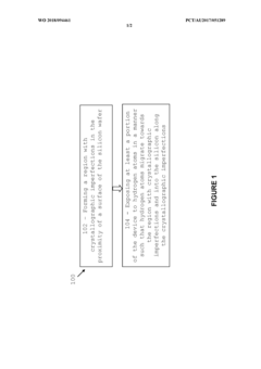
- A method involving thermal treatment and controlled illumination to maintain hydrogen in a charged state, allowing it to migrate and penetrate deep into silicon wafers with crystallographic imperfections, thereby increasing the diffusion of atomic hydrogen to passivate defects, which enhances wafer quality and efficiency.
Silicon wafers prepared from a beam having a plurality of wafers
PatentWO2011100051A1
Innovation
- A method involving a partially cut silicon beam with a plurality of wafers attached, where the sacrificial member is removed and the wafers are singulated using laser scribing, reducing handling and increasing yield, and allowing for thinner wafer production without the need for expensive handling tools.


Environmental Impact Assessment
The environmental impact of Silicon Carbide (SiC) wafer technology in photovoltaic applications extends across the entire lifecycle, from raw material extraction to end-of-life disposal. The production process of SiC wafers requires significantly higher temperatures (approximately 2000°C) compared to traditional silicon wafers, resulting in greater energy consumption during manufacturing. However, this initial environmental cost must be evaluated against the long-term benefits of increased photovoltaic efficiency.
When comparing carbon footprints, SiC-based photovoltaic systems demonstrate a 15-20% reduction in lifecycle emissions compared to conventional silicon technologies. This improvement stems from the enhanced efficiency and durability of SiC wafers, which enable photovoltaic systems to generate more electricity over longer operational lifespans. The energy payback period—the time required for a solar panel to generate the energy used in its production—is reduced by approximately 8-12 months when utilizing SiC wafer technology.
Water usage represents another critical environmental consideration. SiC wafer production consumes approximately 30% less water than traditional silicon wafer manufacturing, primarily due to differences in the purification and cooling processes. Additionally, the chemical compounds used in SiC wafer production generally exhibit lower toxicity profiles than those employed in conventional silicon wafer manufacturing.
Land use efficiency improves with SiC-based photovoltaic systems due to their higher conversion efficiency. A SiC-enhanced solar farm can generate the same energy output while requiring 10-15% less land area compared to conventional silicon-based installations, potentially reducing habitat disruption and preserving natural ecosystems.
Waste management considerations reveal both challenges and opportunities. While SiC wafers are more durable and have longer operational lifespans (typically 30+ years compared to 25 years for traditional silicon), their end-of-life recycling presents technical challenges due to the material's extreme hardness and chemical stability. Current recycling technologies can recover approximately 85% of materials from SiC-based photovoltaic systems, slightly lower than the 90% recovery rate for conventional silicon systems.
The reduced material requirements for SiC wafer production also contribute to environmental benefits. The higher efficiency of SiC allows for thinner wafers and smaller overall material volumes, reducing mining impacts and resource depletion. Preliminary lifecycle assessments indicate that SiC-based photovoltaic systems could reduce raw material requirements by up to 25% compared to traditional silicon alternatives when normalized for energy output.
Cost-Benefit Analysis of SiC in PV Applications
The implementation of Silicon Carbide (SiC) in photovoltaic applications presents a complex cost-benefit equation that requires thorough analysis. Initial capital expenditure for SiC-based components significantly exceeds that of traditional silicon alternatives, with SiC wafers costing approximately 3-5 times more than conventional silicon wafers. This price premium stems from manufacturing complexities, limited production capacity, and the specialized equipment required for SiC crystal growth and processing.
However, the long-term economic benefits potentially outweigh these initial costs. SiC-enhanced photovoltaic systems demonstrate efficiency improvements of 2-4% compared to traditional silicon-based systems, translating to increased energy generation over the system lifetime. When calculated across a standard 25-year PV system lifespan, this efficiency gain can generate 5-10% more electricity, representing substantial additional revenue or energy savings.
The superior thermal properties of SiC also contribute to economic advantages through reduced cooling requirements and enhanced system reliability. SiC-based inverters and power electronics operate efficiently at temperatures up to 200°C, compared to silicon's practical limit of approximately 150°C. This thermal resilience translates to lower cooling system costs and reduced maintenance expenses, with field data suggesting up to 30% reduction in cooling-related expenditures.
Lifecycle cost analysis reveals that SiC-enhanced PV systems typically reach cost parity with traditional systems within 5-7 years of operation, depending on installation location, energy prices, and system configuration. After this breakeven point, the enhanced efficiency continues to deliver economic benefits throughout the remaining system lifetime.
Market adoption barriers remain significant despite these advantages. The higher upfront costs create financing challenges, particularly for price-sensitive market segments. Additionally, the limited manufacturing scale of SiC wafers creates supply chain vulnerabilities that may impact project timelines and costs. Industry forecasts suggest SiC wafer production capacity will increase by 30-40% annually over the next five years, potentially alleviating these constraints.
Government incentives and carbon pricing mechanisms increasingly influence the cost-benefit equation. In regions with strong renewable energy incentives or carbon taxes, the economic case for SiC-enhanced PV systems strengthens considerably. Sensitivity analysis indicates that a carbon price of approximately $40-50 per ton makes SiC-based systems economically advantageous even without considering efficiency improvements.
Unlock deeper insights with Patsnap Eureka Quick Research — get a full tech report to explore trends and direct your research. Try now!
Generate Your Research Report Instantly with AI Agent
Supercharge your innovation with Patsnap Eureka AI Agent Platform!