

Transparent Conductive Oxides: Implications for Industry Standards
OCT 27, 20259 MIN READ
Generate Your Research Report Instantly with AI Agent
PatSnap Eureka helps you evaluate technical feasibility & market potential.
TCO Development History and Objectives
Transparent Conductive Oxides (TCOs) emerged in the early 20th century with the discovery of cadmium oxide's conductive properties in 1907. However, significant development began in the 1940s with tin-doped indium oxide (ITO) research. The 1970s marked a pivotal era as the semiconductor and display industries drove demand for high-performance transparent conductors, establishing ITO as the industry standard due to its exceptional combination of optical transparency and electrical conductivity.
The evolution of TCOs has been characterized by continuous efforts to optimize the fundamental trade-off between transparency and conductivity. Early applications were limited by manufacturing constraints and performance limitations, but advancements in thin-film deposition techniques during the 1980s and 1990s, particularly magnetron sputtering, enabled widespread commercial adoption across multiple industries.
The 2000s witnessed diversification beyond ITO, driven by indium's rising costs and supply concerns. Alternative TCOs including fluorine-doped tin oxide (FTO), aluminum-doped zinc oxide (AZO), and gallium-doped zinc oxide (GZO) emerged as viable alternatives for specific applications. This diversification reflected the maturing understanding of TCO materials science and the ability to engineer properties through doping strategies and deposition parameters.
Recent technological trajectories have focused on developing TCOs compatible with flexible electronics, addressing environmental concerns, and enhancing durability under extreme conditions. Amorphous TCOs have gained prominence for their mechanical flexibility and uniform properties, while research into nanostructured TCOs has opened new possibilities for performance enhancement through quantum effects and surface engineering.
The primary objectives driving TCO development today include reducing reliance on scarce elements like indium, improving compatibility with emerging manufacturing techniques such as roll-to-roll processing, and meeting increasingly stringent performance requirements for next-generation devices. Industry standards have evolved from basic specifications of sheet resistance and visible light transmittance to comprehensive frameworks addressing environmental impact, reliability under various conditions, and integration capabilities.
Looking forward, TCO development aims to achieve higher performance metrics while simultaneously reducing costs and environmental footprint. Specific technical targets include sheet resistances below 10 ohms/square with >90% optical transparency, enhanced durability against mechanical stress and chemical exposure, and compatibility with temperature-sensitive substrates. These objectives align with broader industry trends toward sustainable electronics, flexible devices, and advanced energy technologies that demand exceptional optoelectronic materials.
Market Analysis for Transparent Conductive Materials
The transparent conductive materials market has witnessed substantial growth over the past decade, primarily driven by the expanding electronics industry and increasing demand for touchscreen devices. Currently valued at approximately 5.1 billion USD, this market is projected to grow at a compound annual growth rate (CAGR) of 8.7% through 2028, according to recent industry analyses. Transparent conductive oxides (TCOs), particularly indium tin oxide (ITO), continue to dominate with over 70% market share due to their established manufacturing processes and reliable performance characteristics.
Regional market distribution shows Asia-Pacific leading with nearly 65% of global production capacity, with China, South Korea, and Japan serving as manufacturing hubs. North America and Europe follow with approximately 18% and 12% market shares respectively, focusing primarily on high-end applications and research advancements.
Application segmentation reveals that display technologies consume the largest portion of transparent conductive materials at 58%, followed by photovoltaics (17%), smart windows (12%), and emerging applications including flexible electronics (13%). The smartphone and tablet sector remains the single largest consumer, accounting for approximately 40% of total market volume.
Price sensitivity analysis indicates significant volatility in raw material costs, particularly for indium, which has experienced price fluctuations of up to 30% in recent years. This volatility has accelerated research into alternative materials, creating market opportunities for non-indium based solutions.
Customer demand patterns show increasing requirements for materials with higher transparency (>90%), lower sheet resistance (<10 ohms/square), and enhanced flexibility for next-generation devices. Additionally, sustainability concerns are reshaping purchasing decisions, with 47% of OEMs now including environmental impact assessments in their supplier evaluation processes.
Competitive landscape analysis reveals that while established manufacturers like Nitto Denko, Tosoh Corporation, and JX Nippon Mining & Metals maintain strong positions, emerging players specializing in alternative materials such as silver nanowires, carbon nanotubes, and graphene are gaining traction, collectively capturing approximately 22% of new projects in 2022.
Market barriers include high capital requirements for production facilities, stringent quality control standards, and intellectual property constraints. New entrants typically require 3-5 years to achieve meaningful market penetration, with R&D investments averaging 12-15% of revenue for companies focused on novel transparent conductive materials.
Global TCO Technology Landscape and Barriers
The global landscape of Transparent Conductive Oxide (TCO) technology reveals significant disparities in development and implementation across different regions. Asia, particularly Japan, South Korea, and China, has emerged as the dominant force in TCO research and production, accounting for approximately 60% of global patents in this field. These countries have established robust manufacturing ecosystems that support large-scale production of TCO materials, especially indium tin oxide (ITO), which remains the industry standard despite its limitations.
In North America and Europe, research efforts are more focused on developing alternative TCO materials to address the scarcity and cost issues associated with indium. Academic institutions and technology companies in these regions are pioneering work on zinc oxide-based compounds, fluorine-doped tin oxide (FTO), and aluminum-doped zinc oxide (AZO) as potential replacements for conventional ITO.
The current technological barriers in TCO development present significant challenges for industry-wide adoption. The most pressing issue remains the trade-off between optical transparency and electrical conductivity. While ITO offers excellent performance in both aspects, achieving similar or superior properties with alternative materials has proven difficult. This fundamental challenge has slowed the transition away from indium-dependent technologies.
Material cost and availability constitute another major barrier. Indium's limited supply and fluctuating prices have created market volatility, with prices increasing by over 300% in the past decade. This situation has accelerated research into alternative materials but has also created uncertainty for manufacturers dependent on TCO technologies.
Manufacturing scalability presents additional challenges. Many promising TCO alternatives demonstrate excellent properties in laboratory settings but face significant hurdles in scaling to industrial production. Deposition techniques such as sputtering, chemical vapor deposition, and sol-gel processes each have limitations in terms of uniformity, defect control, and cost-effectiveness at large scales.
Environmental and regulatory barriers are increasingly significant. The extraction and processing of rare elements used in TCOs have substantial environmental impacts, while evolving regulations on hazardous substances in electronics manufacturing are creating compliance challenges for global supply chains.
Interoperability across different TCO technologies remains problematic. The lack of standardized testing protocols and performance metrics makes direct comparisons between different TCO materials difficult, hampering informed decision-making by industry stakeholders and slowing the adoption of innovative solutions.
Current TCO Fabrication and Implementation Methods
01 Composition and structure of transparent conductive oxides
Transparent conductive oxides (TCOs) are materials that combine optical transparency with electrical conductivity. These materials typically consist of metal oxides doped with specific elements to enhance their electrical properties while maintaining transparency. Common TCO compositions include indium tin oxide (ITO), zinc oxide (ZnO), and tin oxide (SnO2). The crystalline structure and composition significantly influence the performance characteristics of these materials, making them suitable for various electronic applications.- Indium-based transparent conductive oxides: Indium-based materials, particularly indium tin oxide (ITO), are widely used as transparent conductive oxides in various electronic applications. These materials offer excellent electrical conductivity while maintaining high optical transparency in the visible spectrum. The formulation and deposition methods of indium-based TCOs can be optimized to achieve specific resistivity and transparency requirements for applications such as touch screens, displays, and photovoltaic devices.
- Alternative TCO materials to replace indium: Due to the scarcity and high cost of indium, alternative transparent conductive oxide materials are being developed. These alternatives include zinc oxide-based compounds (ZnO), aluminum-doped zinc oxide (AZO), and tin oxide-based materials. These materials aim to provide comparable electrical and optical properties to ITO while reducing dependency on rare elements. Research focuses on improving the conductivity and stability of these alternative materials through doping strategies and novel deposition techniques.
- Deposition methods for TCO thin films: Various deposition techniques are employed to create high-quality transparent conductive oxide thin films with optimal properties. These methods include sputtering, chemical vapor deposition (CVD), pulsed laser deposition, and sol-gel processes. Each technique offers different advantages in terms of film quality, uniformity, substrate compatibility, and production scalability. The choice of deposition method significantly impacts the microstructure, electrical conductivity, and optical transparency of the resulting TCO films.
- TCO applications in flexible electronics: Transparent conductive oxides are being adapted for use in flexible and stretchable electronic devices. This requires developing TCO materials and structures that can withstand mechanical deformation while maintaining electrical conductivity and optical transparency. Approaches include creating composite structures, using nanowire networks, developing crack-resistant formulations, and employing low-temperature deposition methods compatible with flexible substrates. These advances enable applications in wearable devices, flexible displays, and conformable solar cells.
- TCO performance enhancement through doping and multilayer structures: The performance of transparent conductive oxides can be significantly enhanced through strategic doping and multilayer architectures. Doping with elements such as aluminum, gallium, or fluorine can improve electrical conductivity without sacrificing optical transparency. Multilayer structures combining different TCO materials or incorporating buffer layers can optimize the trade-off between conductivity and transparency while improving stability and interface properties. These approaches enable tailoring TCO properties for specific application requirements in optoelectronic devices.
02 Deposition methods for transparent conductive oxide films
Various deposition techniques are employed to create thin films of transparent conductive oxides on different substrates. These methods include sputtering, chemical vapor deposition (CVD), pulsed laser deposition, and sol-gel processes. Each technique offers specific advantages in terms of film quality, uniformity, and production efficiency. The deposition parameters such as temperature, pressure, and gas composition significantly affect the resulting film properties, including transparency, conductivity, and adhesion to the substrate.Expand Specific Solutions03 Applications of transparent conductive oxides in electronic devices
Transparent conductive oxides are widely used in various electronic and optoelectronic devices. They serve as essential components in touch screens, liquid crystal displays (LCDs), organic light-emitting diodes (OLEDs), and solar cells. In these applications, TCOs function as transparent electrodes that allow light to pass through while conducting electricity. The specific requirements for TCO properties vary depending on the application, with some devices prioritizing optical transparency while others require higher electrical conductivity or mechanical flexibility.Expand Specific Solutions04 Doping strategies to enhance TCO performance
Doping is a critical approach to enhance the performance of transparent conductive oxides. By introducing specific elements into the oxide matrix, the electrical conductivity can be significantly improved while maintaining optical transparency. Common dopants include aluminum, gallium, and fluorine for zinc oxide, antimony for tin oxide, and tin for indium oxide. The concentration and distribution of dopants within the TCO structure play crucial roles in determining the material's properties, with optimal doping levels varying based on the intended application.Expand Specific Solutions05 Novel TCO materials and composite structures
Research on transparent conductive oxides has expanded to include novel materials and composite structures that offer improved performance or specific functionalities. These innovations include multi-layered TCO structures, nanocomposites, and alternative materials designed to replace conventional TCOs like indium tin oxide. Some approaches focus on developing indium-free alternatives to address cost and supply concerns, while others aim to create flexible TCOs for next-generation flexible electronics. These novel materials often combine different oxides or incorporate additional elements to achieve unique property combinations.Expand Specific Solutions
Leading TCO Manufacturers and Research Institutions
The transparent conductive oxides (TCO) market is currently in a growth phase, driven by increasing demand in display technologies, photovoltaics, and smart devices. The global market size is estimated to reach $8.5 billion by 2026, with a CAGR of approximately 6.8%. Technologically, the field shows varying maturity levels across applications. Industry leaders like Applied Materials, TDK, and Micron Technology are advancing commercial applications, while research institutions such as Peking University and Oxford University Innovation are pioneering next-generation materials. Companies including AGC, Idemitsu Kosan, and Solvay are developing specialized formulations for emerging applications. The competitive landscape is characterized by a balance between established manufacturers focusing on production efficiency and newcomers exploring novel materials like carbon nanotube alternatives (Eikos, Cambrios) to address TCO limitations.
Applied Materials, Inc.
Technical Solution: Applied Materials has developed advanced Physical Vapor Deposition (PVD) systems specifically optimized for TCO fabrication, including their Endura® platform that enables precise control over film stoichiometry and microstructure. Their technology focuses on indium tin oxide (ITO) and emerging alternatives like indium zinc oxide (IZO) and aluminum-doped zinc oxide (AZO). The company's TCO solutions incorporate multi-chamber processing that allows for in-situ doping and interface engineering to achieve carrier concentration optimization without compromising optical transparency. Their proprietary rotary target technology enables uniform deposition across large substrates with thickness variation below 1.5%, critical for display manufacturing. Applied Materials has also pioneered low-temperature TCO deposition processes (below 100°C) that maintain conductivity while enabling compatibility with flexible substrates and temperature-sensitive device architectures.
Strengths: Industry-leading deposition uniformity across large substrates; comprehensive process control for optimizing electrical-optical trade-offs; established supply chain integration. Weaknesses: Higher capital equipment costs compared to solution-based methods; reliance on indium in many formulations despite supply chain concerns; energy-intensive vacuum-based processes.
Sumitomo Metal Mining Co. Ltd.
Technical Solution: Sumitomo Metal Mining has developed advanced TCO materials focusing on indium-based formulations with enhanced performance characteristics. Their ITOSTAR® product line features ultra-smooth ITO films with surface roughness below 1nm RMS while maintaining sheet resistance under 15 ohms/square and transparency above 90%. The company employs a proprietary sputtering process with precise oxygen partial pressure control that optimizes the trade-off between carrier concentration and mobility. Their technology includes gradient-doped TCO structures that enhance interface properties in multilayer device architectures. Sumitomo has also pioneered indium-saving TCO formulations that reduce indium content by up to 30% through partial substitution with zinc and tin while maintaining comparable performance. Their recent innovations include damage-resistant TCO formulations with enhanced mechanical durability through nanocomposite structures and stress-relief mechanisms, allowing their TCOs to withstand mechanical stresses in flexible display manufacturing.
Strengths: Exceptional film quality with industry-leading surface smoothness; tight process control for batch-to-batch consistency; established supply relationships with major display manufacturers. Weaknesses: Continued reliance on indium despite supply chain concerns; higher production costs compared to some emerging alternatives; limited flexibility compared to nanowire-based solutions.
Key Patents and Breakthroughs in TCO Technology
Sputter Deposition and Annealing of High Conductivity Transparent Oxides
PatentInactiveUS20120160663A1
Innovation
- The use of sputtering techniques with radio frequency energy and optional direct current energy to deposit tin-oxide films at low temperatures (below 100°C) with controlled inert and halogen gas introduction, allowing for smooth, high-conductivity films without surface defects and minimizing energy expenditure.


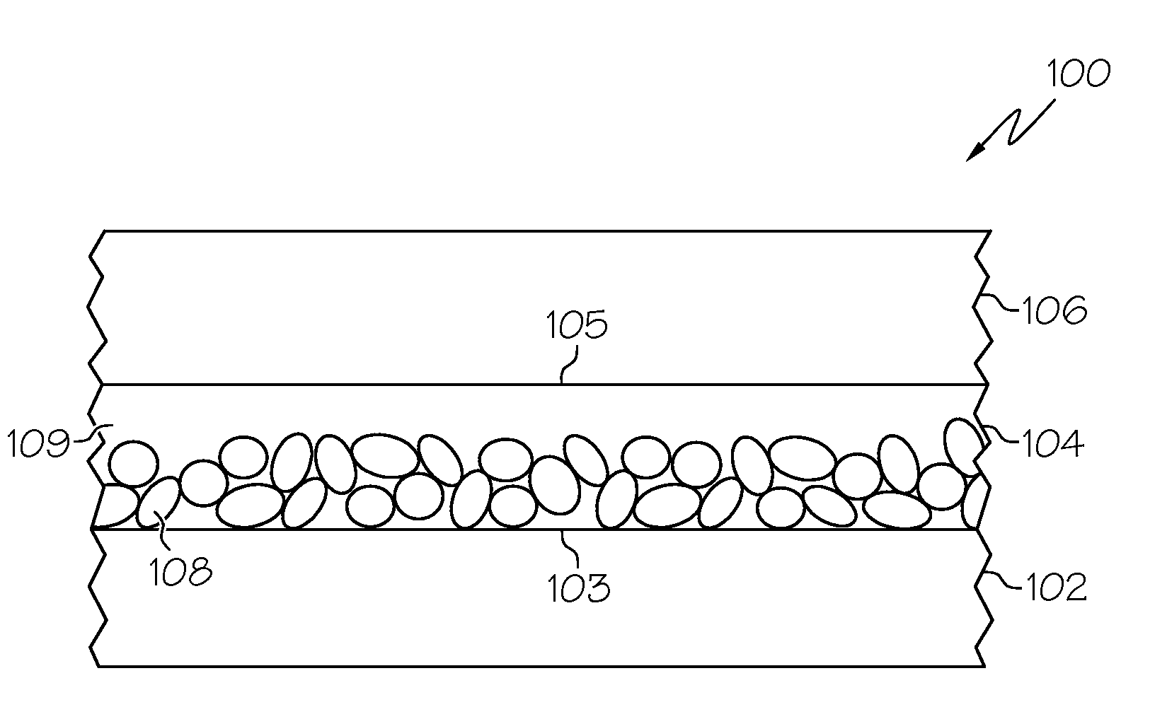
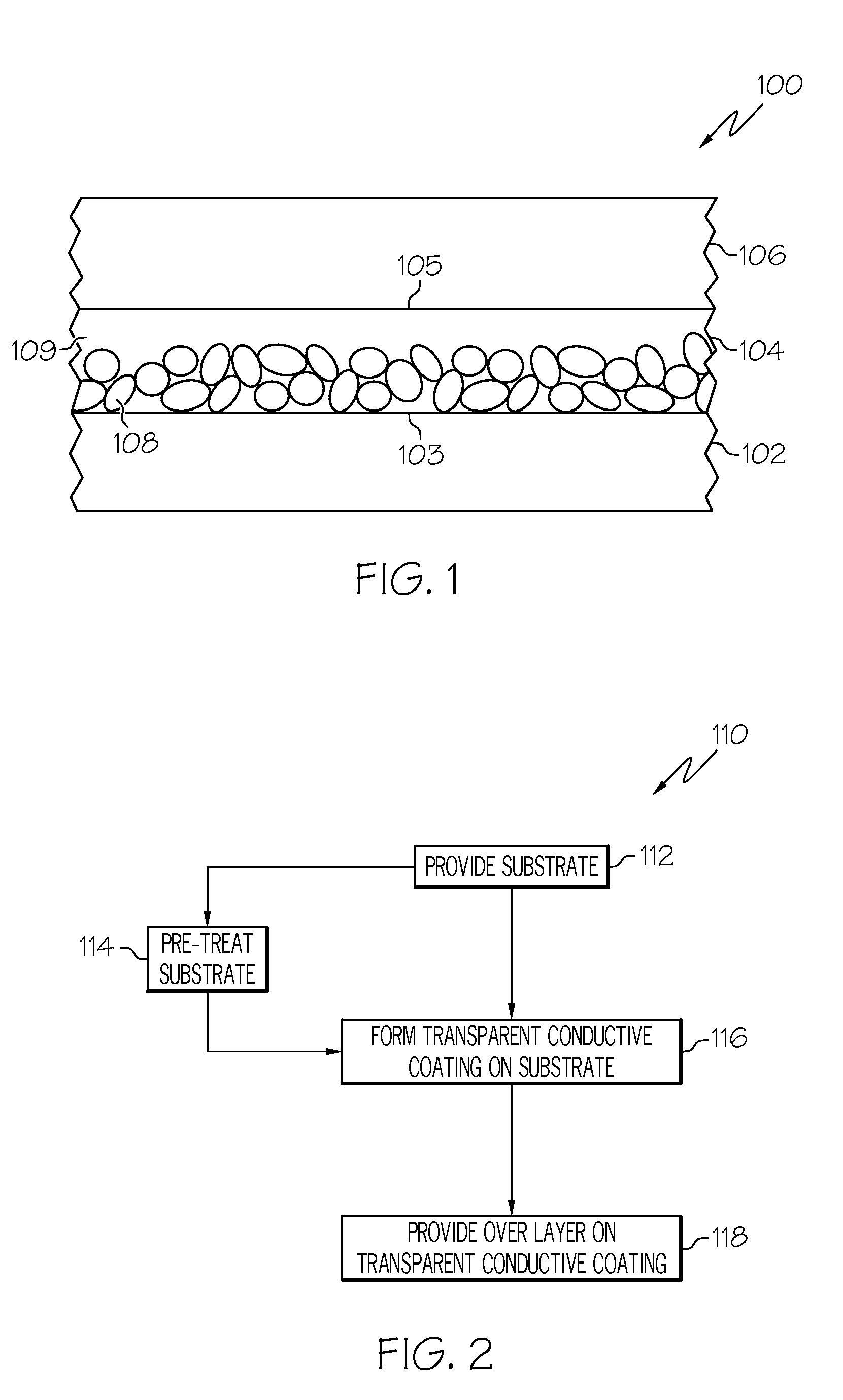
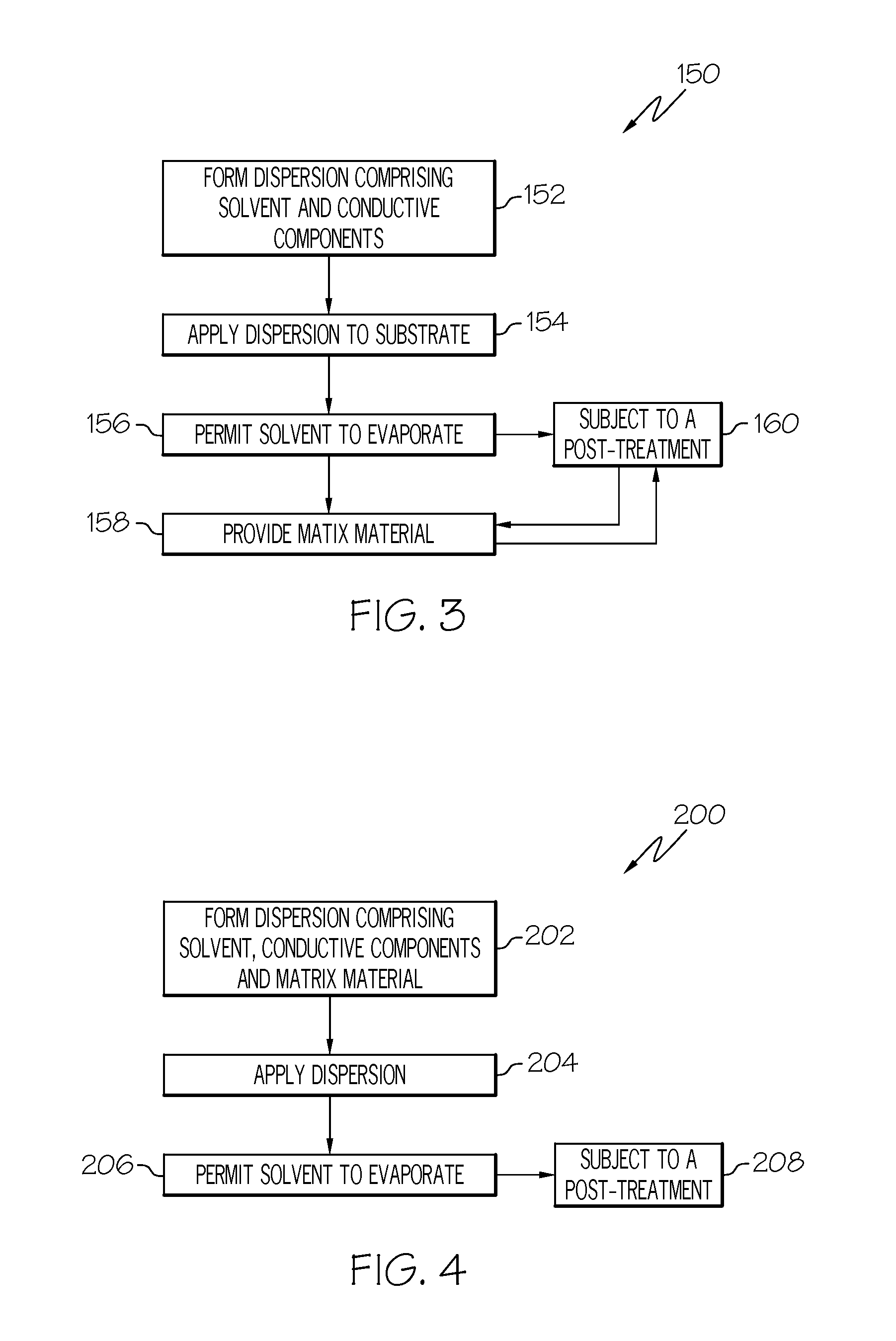
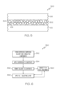
Transparent conductors that exhibit minimal scattering, methods for fabricating the same, and display devices comprising the same
PatentInactiveUS20090191389A1
Innovation
- A transparent conductor configuration with a substrate, a conductive coating, and an over layer, where the conductive coating's refractive index is optimized between the substrate and over layer's indices, minimizing scattering and enhancing transmissivity through a quarter-wave layer design or refractive index-adjusting materials.
Standardization Frameworks for TCO Materials
The standardization of Transparent Conductive Oxide (TCO) materials represents a critical framework for ensuring consistency, reliability, and interoperability across various industries. Currently, several international organizations lead TCO standardization efforts, including the International Electrotechnical Commission (IEC), International Organization for Standardization (ISO), and ASTM International. These bodies have established comprehensive guidelines addressing electrical resistivity, optical transparency, chemical composition, and mechanical durability of TCO materials.
Key standardization parameters for TCOs include sheet resistance (measured in ohms per square), optical transmittance (typically >80% in visible spectrum), haze factor, work function, and environmental stability metrics. These parameters form the foundation of quality assessment protocols that manufacturers must adhere to when producing TCO-based components for electronics, photovoltaics, and display technologies.
The evolution of TCO standards has been marked by progressive refinement, moving from basic electrical and optical specifications toward more sophisticated requirements addressing nanoscale properties, interface characteristics, and long-term reliability. Recent developments have introduced standards specifically for flexible TCO applications, recognizing the growing importance of bendable electronics and displays.
Industry-specific adaptations of TCO standards have emerged to address unique requirements. For instance, photovoltaic applications emphasize different performance metrics compared to touch-screen displays, necessitating specialized certification protocols. The solar industry has developed particular standards focusing on TCO stability under prolonged UV exposure and thermal cycling conditions.
Harmonization efforts between regional standards bodies have accelerated in recent years, with initiatives to align European (EN), American (ANSI), and Asian (JIS, KS) specifications for TCO materials. This convergence aims to reduce trade barriers and streamline global supply chains for TCO-based products.
Emerging standardization frontiers include protocols for next-generation TCO materials such as carbon-based alternatives and hybrid organic-inorganic conductors. Additionally, sustainability metrics are being incorporated into newer standards, evaluating TCO materials based on embodied carbon, recyclability, and reduced dependence on scarce elements like indium.
Compliance verification mechanisms have also evolved, with third-party certification becoming increasingly important for market access. Testing methodologies have been standardized to ensure reproducible measurements across different laboratories, with round-robin testing programs validating measurement consistency across international facilities.
Environmental Impact and Sustainability of TCO Production
The production of Transparent Conductive Oxides (TCOs) presents significant environmental challenges that warrant careful consideration as industry standards continue to evolve. Traditional TCO manufacturing processes, particularly those involving Indium Tin Oxide (ITO), consume substantial energy and utilize scarce raw materials. Indium, a key component in ITO, faces critical supply constraints with reserves projected to deplete within 20-30 years at current consumption rates, raising serious sustainability concerns.
Manufacturing processes for TCOs typically involve energy-intensive sputtering techniques performed under vacuum conditions, contributing to considerable carbon footprints. The high-temperature annealing processes required for optimal conductivity further exacerbate energy consumption issues. Additionally, the etching processes employed in TCO patterning often utilize hazardous chemicals including strong acids and heavy metals, posing environmental contamination risks if not properly managed.
Waste management represents another critical environmental challenge in TCO production. The industry generates significant amounts of material waste during deposition processes, with utilization efficiencies sometimes falling below 30%. This inefficiency not only increases production costs but also compounds the sustainability issues associated with rare element consumption. Furthermore, end-of-life disposal of TCO-containing devices presents recycling challenges due to the difficulty in separating these thin-film materials from their substrates.
Recent sustainability initiatives have focused on developing alternative TCO materials with reduced environmental impacts. Zinc-based compounds such as Aluminum-doped Zinc Oxide (AZO) and Gallium-doped Zinc Oxide (GZO) offer promising alternatives utilizing more abundant elements. Additionally, carbon-based alternatives including graphene and carbon nanotube networks are emerging as potential replacements that could significantly reduce the environmental footprint of transparent conductors.
Life cycle assessment (LCA) studies indicate that the environmental impact of TCOs extends beyond production to include extraction, processing, and disposal phases. Comprehensive LCA frameworks are increasingly being incorporated into industry standards to ensure environmental considerations are systematically addressed throughout the product lifecycle. These assessments typically evaluate multiple impact categories including global warming potential, resource depletion, acidification, and human toxicity.
Regulatory frameworks governing TCO production are evolving globally, with particular emphasis on reducing hazardous substance usage and improving recycling rates. The European Union's Restriction of Hazardous Substances (RoHS) and Waste Electrical and Electronic Equipment (WEEE) directives have significant implications for TCO manufacturers, requiring careful consideration of material selection and end-of-life management strategies. Similar regulatory trends are emerging in North America and Asia, signaling a global shift toward more environmentally responsible TCO production practices.
Unlock deeper insights with PatSnap Eureka Quick Research — get a full tech report to explore trends and direct your research. Try now!
Generate Your Research Report Instantly with AI Agent
Supercharge your innovation with PatSnap Eureka AI Agent Platform!