

What Challenges Do EUV Lithography Processes Face Today
OCT 14, 20259 MIN READ
Generate Your Research Report Instantly with AI Agent
PatSnap Eureka helps you evaluate technical feasibility & market potential.
EUV Lithography Evolution and Objectives
Extreme Ultraviolet (EUV) lithography represents a revolutionary advancement in semiconductor manufacturing, marking a significant departure from traditional optical lithography techniques. The technology's development journey spans over three decades, beginning in the 1980s with initial research into short-wavelength lithography solutions. The fundamental breakthrough came with the adoption of 13.5nm wavelength light, enabling the creation of significantly smaller semiconductor features than previously possible with deep ultraviolet (DUV) systems.
The evolution of EUV technology has been characterized by persistent engineering challenges and collaborative industry efforts. Early development phases focused primarily on creating viable EUV light sources, with laser-produced plasma (LPP) technology eventually emerging as the dominant approach. By the early 2000s, the semiconductor industry recognized EUV as the most promising next-generation lithography solution, leading to increased investment and research coordination through consortia like ASML, Carl Zeiss, and Cymer.
A critical milestone occurred in 2018 when ASML delivered the first commercial EUV lithography systems capable of high-volume manufacturing, enabling the 7nm process node. This achievement represented the culmination of decades of research and billions in investment across the semiconductor ecosystem. The technology has since enabled progression to 5nm nodes, with roadmaps extending to 3nm and beyond.
The primary objective of EUV lithography development has been to maintain the trajectory of Moore's Law by enabling continued miniaturization of semiconductor components. Specific technical goals include achieving resolution below 10nm, improving throughput to economically viable levels (currently targeting >125 wafers per hour), and enhancing yield through better process control and reduced defectivity.
Current EUV development objectives focus on several key areas: increasing source power to improve throughput, developing more sensitive photoresists with improved line edge roughness, creating more efficient optical systems, and implementing advanced computational lithography techniques. High-numerical aperture (High-NA) EUV systems represent the next evolutionary step, promising resolution improvements of approximately 70% over current systems.
The technology aims to support semiconductor scaling for at least another decade, enabling more powerful and energy-efficient electronic devices across computing, communications, automotive, and emerging AI applications. As the industry progresses toward atomic-scale features, EUV lithography stands as the critical enabler of continued semiconductor advancement, though researchers are already exploring potential successor technologies for the post-EUV era.
Semiconductor Industry Demand Analysis
The semiconductor industry's demand for advanced lithography technologies, particularly EUV (Extreme Ultraviolet) lithography, is primarily driven by the relentless pursuit of Moore's Law. As transistor densities continue to increase, the market requires manufacturing processes capable of producing increasingly smaller feature sizes with higher precision and yield rates.
Market analysis indicates that the global semiconductor industry is projected to reach over $600 billion by 2025, with advanced node manufacturing representing a significant growth segment. The demand for EUV lithography systems stems from leading-edge semiconductor manufacturers producing chips at 7nm nodes and below, where traditional DUV (Deep Ultraviolet) lithography reaches its physical limitations.
The transition to EUV lithography is accelerated by consumer demand for higher-performance computing devices, artificial intelligence applications, and data centers. These applications require chips with greater transistor densities, lower power consumption, and higher performance - all benefits that EUV technology can potentially deliver through its ability to pattern smaller features.
Mobile device manufacturers represent another significant market driver, as they continuously seek more powerful and energy-efficient processors for smartphones and tablets. The automotive sector is also emerging as a key demand source, with advanced driver-assistance systems and autonomous driving technologies requiring sophisticated semiconductor components that benefit from EUV-enabled manufacturing processes.
Industry trends indicate that while only a handful of semiconductor manufacturers currently implement EUV lithography in production, the technology adoption curve is steepening. Taiwan, South Korea, and the United States lead in EUV implementation, with China actively seeking to develop domestic capabilities despite export control challenges.
The economic implications of EUV adoption are substantial, with each lithography system representing an investment exceeding $150 million. This high capital expenditure creates a significant barrier to entry, concentrating advanced manufacturing capabilities among a small number of global players.
From a supply chain perspective, the limited number of EUV equipment suppliers (primarily ASML as the sole manufacturer of production-grade EUV lithography systems) creates potential bottlenecks in meeting industry demand. This supply constraint is compounded by the complex nature of the technology and the specialized materials required for EUV processes, including specialized photoresists and mask technologies.
Looking forward, market forecasts suggest that EUV lithography will become increasingly essential for competitive semiconductor manufacturing, with the technology expected to penetrate deeper into the semiconductor value chain as costs gradually decrease and technical challenges are overcome.
EUV Technical Barriers and Global Development Status
Extreme Ultraviolet (EUV) lithography represents a revolutionary advancement in semiconductor manufacturing, enabling the production of increasingly smaller transistors and more powerful integrated circuits. However, this cutting-edge technology faces significant technical barriers that impede its widespread adoption and optimal performance.
The most pressing challenge for EUV lithography is power source limitations. Current EUV light sources struggle to generate sufficient power for high-volume manufacturing, resulting in reduced throughput and increased production costs. The industry standard of 250W source power remains difficult to maintain consistently, with frequent fluctuations affecting exposure quality and production efficiency.
Photoresist performance presents another critical barrier. EUV photoresists must simultaneously achieve high sensitivity, low line edge roughness (LER), and minimal pattern collapse at extremely small dimensions. This "triangle of death" trade-off continues to challenge material scientists, as improvements in one parameter often come at the expense of others, limiting overall lithographic performance.
Mask defectivity remains a persistent obstacle. EUV masks are particularly susceptible to defects due to their complex multilayer structure and the absence of pellicles in early implementations. Even nanometer-scale defects can cause critical pattern failures, while inspection and repair technologies struggle to keep pace with increasingly stringent requirements.
Stochastic effects have emerged as a fundamental physical limitation. At extreme dimensions, random variations in photon absorption and chemical reactions lead to unpredictable pattern defects. These stochastic failures increase exponentially as feature sizes decrease, potentially setting a physical limit to further scaling using current EUV approaches.
Globally, EUV development shows distinct regional patterns. The Netherlands dominates equipment manufacturing through ASML's monopoly on EUV scanners. The United States leads in computational lithography and design solutions, while Japan excels in materials development, particularly photoresists and mask blanks. South Korea and Taiwan have established themselves as primary implementers, integrating EUV into high-volume manufacturing environments.
China faces significant barriers to EUV adoption due to export restrictions, forcing alternative technology paths. Meanwhile, European research institutions continue to advance fundamental EUV science through consortia like IMEC. This geographic distribution of expertise creates both collaboration opportunities and geopolitical tensions that further complicate EUV's technical advancement.
The economic barriers to EUV adoption remain substantial, with each scanner costing over $150 million and requiring extensive supporting infrastructure. This limits adoption to only the largest semiconductor manufacturers, creating a widening technological gap in the industry.
Current EUV Process Solutions and Implementations
01 Contamination control in EUV lithography systems
Contamination is a significant challenge in EUV lithography systems. Particles and molecular contaminants can degrade the performance of optical components and reduce the quality of the lithographic process. Various methods have been developed to address this issue, including specialized cleaning techniques, contamination barriers, and monitoring systems to detect and mitigate contamination before it affects the lithography process.- Contamination control in EUV lithography systems: Contamination is a significant challenge in EUV lithography systems. Particles and molecular contaminants can degrade the performance of optical components and reduce the quality of the lithographic process. Various methods have been developed to address this issue, including specialized cleaning techniques, contamination barriers, and monitoring systems to detect and mitigate contamination in real-time. These approaches help maintain the integrity of the EUV optical path and ensure consistent lithographic performance.
- Thermal management in EUV systems: EUV lithography systems generate significant heat during operation, which can lead to thermal expansion, distortion of optical components, and degradation of system performance. Effective thermal management strategies are essential to maintain the precision required for nanometer-scale lithography. These include advanced cooling systems, temperature-stabilized environments, and thermal compensation mechanisms that adjust for heat-induced changes in the optical path. Proper thermal management is critical for achieving consistent exposure quality and system reliability.
- Mask defectivity and inspection challenges: EUV masks are highly complex and susceptible to various types of defects that can impact pattern transfer quality. Challenges include detecting sub-nanometer defects, distinguishing between harmful and harmless defects, and developing repair technologies. Advanced inspection tools using multiple illumination techniques are needed to identify defects that would be printable in the lithography process. Additionally, pellicle development for EUV masks presents unique challenges due to the high energy of EUV radiation and the need for extremely thin, yet robust protective films.
- Source power and stability issues: EUV light sources face significant challenges in achieving sufficient power output for high-volume manufacturing while maintaining stability. Laser-produced plasma (LPP) sources, which generate EUV radiation by targeting droplets of tin with high-power lasers, must balance power output with consistent droplet generation, targeting accuracy, and debris mitigation. Innovations in source design focus on improving conversion efficiency, enhancing collector mirror lifetime, and developing sophisticated feedback systems to maintain stable output over extended operation periods.
- Optical system design and alignment: EUV lithography requires complex optical systems with extremely precise alignment tolerances. The all-reflective optical design using multilayer mirrors presents unique challenges in maintaining positioning accuracy at the picometer level. Advanced metrology systems are needed for initial alignment and continuous monitoring during operation. Adaptive optics technologies help compensate for small deviations in real-time. Additionally, the optical system must be designed to minimize flare and other aberrations that can degrade image quality at the nanometer scale.
02 Thermal management in EUV systems
EUV lithography systems generate significant heat during operation, which can cause thermal expansion and distortion of critical components. This thermal instability affects the precision of the lithographic process. Advanced thermal management solutions include cooling systems, temperature-controlled environments, and materials with low thermal expansion coefficients to maintain the stability and accuracy of the EUV lithography system during operation.Expand Specific Solutions03 Mask defect inspection and repair
EUV masks are highly susceptible to defects that can significantly impact the final pattern quality. Detecting and repairing these defects is challenging due to the small feature sizes and complex patterns involved in EUV lithography. Advanced inspection tools and repair techniques have been developed to identify and correct defects on EUV masks, ensuring the accuracy and reliability of the lithographic process.Expand Specific Solutions04 Source power and stability challenges
EUV light sources face challenges in achieving sufficient power output and stability for high-volume manufacturing. Low source power leads to reduced throughput, while instability affects pattern quality. Innovations in plasma generation, collector design, and power delivery systems aim to enhance the power and stability of EUV sources, improving the efficiency and reliability of EUV lithography systems.Expand Specific Solutions05 Optical system design and alignment
EUV lithography requires complex optical systems with multiple reflective elements that must be precisely aligned and maintained. Challenges include minimizing wavefront errors, managing flare, and maintaining alignment during operation. Advanced metrology systems and adaptive optics have been developed to address these challenges, ensuring the optical performance necessary for high-resolution EUV lithography.Expand Specific Solutions
Leading EUV Equipment Manufacturers and Ecosystem
EUV lithography processes face significant challenges in today's semiconductor manufacturing landscape. The industry is in a mature growth phase with the global EUV lithography market expected to reach $10-15 billion by 2025. Technical challenges include pattern fidelity issues, stochastic effects, and photoresist sensitivity limitations. Leading players like TSMC, Intel, and Samsung are investing heavily in overcoming these barriers, while equipment manufacturers such as ASML (the sole EUV lithography system provider) work closely with materials companies like Shin-Etsu Chemical and JSR to develop advanced photoresists. Research institutions including IMEC and universities collaborate with industry to solve fundamental physics challenges related to source power, mask defects, and throughput limitations that currently constrain wider EUV adoption across more semiconductor manufacturing nodes.
Taiwan Semiconductor Manufacturing Co., Ltd.
Technical Solution: TSMC has developed a comprehensive EUV lithography implementation strategy focusing on high-volume manufacturing readiness. Their approach includes custom-designed EUV photoresist materials with optimized sensitivity and resolution characteristics, advanced pellicle technologies to protect masks from contamination, and sophisticated computational lithography techniques. TSMC has successfully implemented EUV in their 7nm+ and 5nm process nodes, achieving critical dimension uniformity below 2nm. Their EUV implementation includes specialized metrology systems for defect inspection and has demonstrated yield improvements of approximately 20% compared to multi-patterning DUV approaches. TSMC has also developed proprietary solutions for stochastic effects mitigation through mask optimization algorithms and process control methodologies that reduce line edge roughness by up to 30%.
Strengths: Industry-leading EUV implementation with proven high-volume manufacturing capability; advanced computational lithography expertise; comprehensive defect control systems. Weaknesses: High capital expenditure requirements; dependency on limited EUV equipment suppliers; ongoing challenges with throughput optimization at advanced nodes.
SAMSUNG SDI CO LTD
Technical Solution: Samsung has developed a comprehensive EUV lithography strategy centered on their semiconductor manufacturing processes. Their approach includes proprietary photoresist formulations with enhanced sensitivity characteristics, achieving approximately 30% improvement in exposure latitude compared to early EUV materials. Samsung has implemented advanced mask inspection and qualification protocols to address pattern fidelity challenges, with automated systems capable of detecting defects below 20nm. Their EUV implementation includes sophisticated computational lithography techniques with machine learning algorithms that predict and compensate for stochastic effects, reducing line edge roughness by up to 25%. Samsung has successfully deployed EUV in their 7nm and 5nm production nodes, with ongoing research focused on extending EUV capabilities to 3nm and beyond. Their strategy includes specialized process control methodologies that optimize dose and focus parameters in real-time, maintaining critical dimension uniformity across wafers.
Strengths: Extensive experience with high-volume EUV manufacturing; vertically integrated approach from materials to process; advanced computational solutions for stochastic effects. Weaknesses: High capital intensity requirements; ongoing challenges with EUV source power stability; throughput limitations at most advanced nodes.
Critical EUV Patents and Technical Innovations
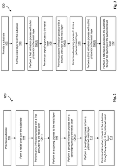
Extreme ultraviolet photolithography method with infiltration for enhanced sensitivity and etch resistance
PatentActiveUS12111576B2
Innovation
- Incorporating a metal-containing chemical into the photoresist through an infiltration process, such as atomic layer deposition or chemical vapor deposition, to enhance EUV sensitivity and etch resistance, allowing the photoresist to be more effective under EUV radiation and improve patterning accuracy.

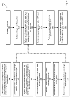

Extreme ultraviolet lithography process
PatentActiveUS20160377983A1
Innovation
- The EUV lithography process employs an illuminator that sets the chief ray angle of incidence (CRAO) to less than three degrees, removing more than 70% of non-diffracted light and utilizing balanced diffracted light orders to enhance image contrast and resolution, thereby minimizing shadowing effects and relaxing thickness constraints.


Supply Chain Vulnerabilities in EUV Ecosystem
The EUV lithography ecosystem presents significant supply chain vulnerabilities that threaten the stability and advancement of semiconductor manufacturing. At the core of these vulnerabilities is the extreme concentration of critical components and expertise. ASML, headquartered in the Netherlands, maintains a near-monopoly on EUV lithography systems, creating a single point of failure in the global semiconductor supply chain. This concentration risk is further exacerbated by the fact that ASML relies on a limited number of specialized suppliers for critical subsystems.
The optical components, particularly the complex mirror systems required for EUV lithography, face severe supply constraints. Zeiss, as the sole provider of these sophisticated mirror systems, creates another bottleneck in the supply chain. The manufacturing process for these mirrors requires exceptional precision and specialized materials, with limited production capacity worldwide.
Raw material dependencies present another layer of vulnerability. EUV systems require specific rare earth elements and specialized materials that often originate from geopolitically sensitive regions. The limited geographical distribution of these resources creates exposure to trade restrictions, political tensions, and natural disasters that could disrupt supply.
Geopolitical tensions have increasingly impacted the EUV ecosystem, with export controls and technology restrictions between major semiconductor-producing nations creating uncertainty. The strategic importance of semiconductor technology has led to nationalistic policies that fragment the global supply chain, potentially limiting access to critical EUV technology for certain markets.
Manufacturing capacity constraints further compound these vulnerabilities. The production of EUV systems involves highly specialized equipment and expertise, with limited manufacturing facilities worldwide. ASML's production capacity cannot easily scale to meet rapidly growing demand, creating extended lead times that can exceed 18 months for new EUV systems.
Workforce limitations represent another critical vulnerability. The development and maintenance of EUV systems require highly specialized engineers and technicians with expertise in optics, vacuum systems, and precision mechanics. This talent pool is limited globally and concentrated in specific regions, creating competition for skilled personnel.
The interdependence between EUV suppliers and semiconductor manufacturers creates mutual vulnerabilities. Disruptions at any point in this complex ecosystem can cascade throughout the supply chain, affecting multiple stakeholders and potentially causing production delays across the semiconductor industry.
Environmental Impact and Sustainability Challenges
EUV lithography processes, while revolutionary for semiconductor manufacturing, present significant environmental and sustainability challenges that the industry must address. The manufacturing and operation of EUV systems consume substantial energy resources, with a single EUV lithography machine requiring up to 1 MW of power during operation. This energy-intensive process contributes significantly to the carbon footprint of semiconductor fabrication facilities, raising concerns about long-term sustainability in an increasingly climate-conscious global economy.
Water usage represents another critical environmental challenge. EUV lithography requires ultra-pure water for cleaning processes, with estimates suggesting that a typical semiconductor fabrication facility may consume millions of gallons of water daily. In regions facing water scarcity, this intensive consumption pattern raises serious sustainability questions and potential regulatory challenges.
The chemical waste generated by EUV processes presents additional environmental concerns. Various chemicals used in photoresist development, etching, and cleaning processes can produce hazardous waste streams that require specialized treatment and disposal. These include perfluorinated compounds and other persistent chemicals that may have long-term environmental impacts if not properly managed.
Resource scarcity also emerges as a sustainability challenge for EUV lithography. The technology relies on rare materials, particularly for the fabrication of specialized mirrors and other components. The limited availability of these materials raises questions about supply chain resilience and the long-term viability of scaling EUV technology to meet growing semiconductor demand.
Regulatory compliance represents an evolving challenge as environmental standards become increasingly stringent worldwide. Semiconductor manufacturers must navigate complex and sometimes conflicting regulatory frameworks across different regions, adding complexity to global manufacturing strategies and potentially increasing compliance costs.
The industry has begun responding to these challenges through various initiatives. These include developing more energy-efficient EUV systems, implementing water recycling technologies, researching alternative chemicals with reduced environmental impact, and exploring circular economy approaches to material recovery and reuse. However, significant research and development investments will be required to address these environmental and sustainability challenges while maintaining the technological advantages that EUV lithography provides to semiconductor manufacturing.
Unlock deeper insights with PatSnap Eureka Quick Research — get a full tech report to explore trends and direct your research. Try now!
Generate Your Research Report Instantly with AI Agent
Supercharge your innovation with PatSnap Eureka AI Agent Platform!